
PCB Materials and Surface Finishes: FR4, Rogers and PTFE Guide
Compare FR4, high-Tg FR4, Rogers and PTFE PCB materials, plus ENIG, HASL, OSP, immersion silver and tin finishes for high-frequency manufacturing.
PTFE PCB Manufacturing Specifications: A Practical Fabrication Example
Explore PTFE PCB manufacturing specifications, laminate selection, copper thickness, drilling, ENIG surface finish and a practical bare-board fabrication example.
PCB Manufacturing Requirements: Complete Fabrication Checklist
Learn essential PCB manufacturing requirements, including Gerber files, copper thickness, drill tolerances, impedance control, panelization and surface finishes.
PCB Stack-Up Design Guide: How High-Speed and High-Frequency PCBs Ensure Performance from the Structure
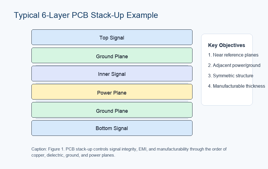
PCB Stack-Up Design Guide: How High-Speed and High-Frequency PCBs Ensure Performance from the Structure PCB stack-up design coordinates conductive and dielectric layers to support controlled impedance, predictable return paths, power distribution, and practical PCB fabrication. This guide focuses on design principles and includes a real six-layer Rogers RO4350B stack-up example. Table of Contents What Is […]
Choosing the Right Material for Your RF PCB Designs
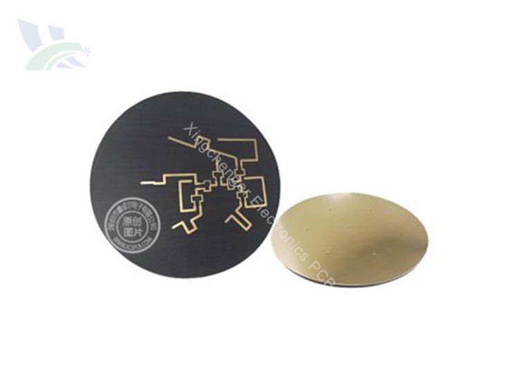
RF PCB Material Selection: FR4 vs Rogers vs PTFE Table of Contents RF PCB material selection is one of the earliest decisions in high-frequency circuit design. Many RF designs begin on standard FR-4 because of its availability and cost advantages, but as operating frequency increases, material properties start having a greater impact on performance. The […]
6 Tips for Selecting RF and Microwave PCB Materials

6 Tips for Selecting RF and Microwave PCB Materials Selecting the right PCB material for an RF or microwave design is one of those decisions that shows up in every measurement afterwards. High-frequency circuits leave little margin — signal loss, phase drift and unstable electrical properties all trace back to the laminate. The six tips […]
RO3003 Bond vs RO4450: Differences, Lamination Process, and Best Bonding Material for Rogers RO3003 PCB
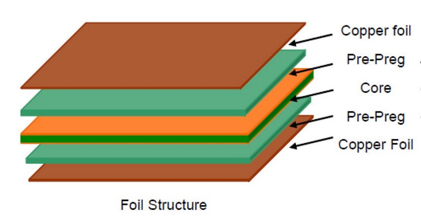
RO3003 Bond vs RO4450: Differences, Lamination Process, and Best Bonding Material for Rogers RO3003 PCB Designing multilayer RF and microwave PCBs takes more than picking a low-loss substrate. One question comes up again and again: can Rogers RO3003 laminates be pressed together directly, without a bonding material? The answer is no — and it’s worth […]
FR-4 vs Rogers PCB Materials: Cost, Supply Chain, and High Frequency Market Reality
Learn fr 4 vs rogers pcb materials cost supply chain and high frequency market reality with practical guidance on materials, stackup, process control and RF p
High-Frequency Multilayer PCB Manufacturing Process: Key Challenges and Quality Control for 5G and RF Applications
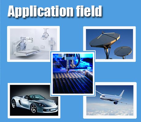
High-Frequency Multilayer PCB Manufacturing Process: Key Challenges and Quality Control for 5G and RF Applications High-frequency multilayer PCBs carry GHz-level signals in 5G base stations, automotive radar, satellite payloads and aerospace electronics. Compared with a standard FR-4 board, nothing about the process is forgiving: Dk has to stay stable, Df has to stay low, impedances […]
PCB Stackup Design Guide: Best Practices for 4-Layer, 6-Layer, and 8-Layer PCBs
PCB Stackup Design Guide: Best Practices for 4-Layer, 6-Layer, and 8-Layer PCBs Stackup decisions sit upstream of everything: signal integrity, EMC, impedance control, power distribution. Yet a lot of designers pour their energy into routing, component placement and decoupling capacitors, and treat the stackup as a detail to settle later. That’s backwards — a poor […]
High-Frequency PCB Surface Finishes Compared: ENIG vs Silver vs Tin for RF and Microwave Applications
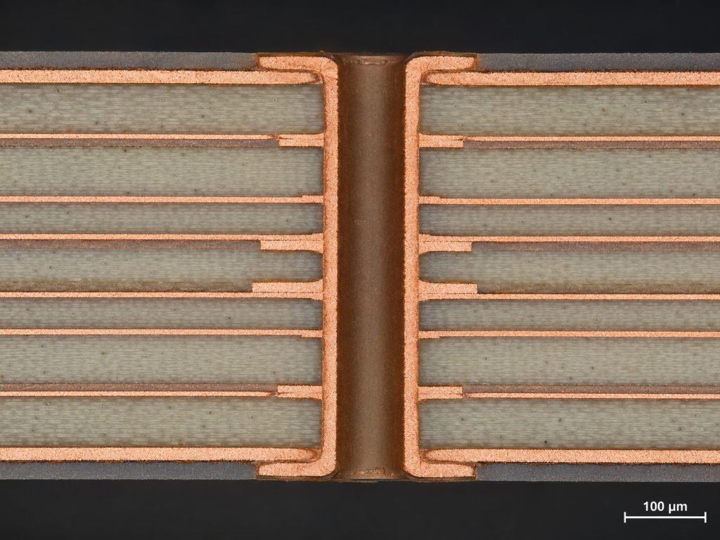
High-Frequency PCB Surface Finishes Compared: ENIG vs Silver vs Tin for RF and Microwave Applications ENIG, immersion silver and immersion tin compared on insertion loss, surface roughness and RF reliability — so you can pick the right finish for your frequency band. Table of Contents High-Frequency PCB Surface Finishes Compared: ENIG vs Silver vs Tin […]
How to solve the problems of compression alignment and expansion/contraction?
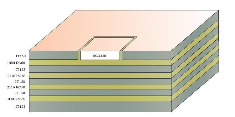
How to Solve Compression Alignment and Expansion/Contraction Problems in High-Frequency Multilayer PCBs Why RF multilayer boards drift during lamination — and how artwork compensation, precision positioning, mixed-material lamination control and LDI imaging hold registration within ±25 µm. Table of Contents In high frequency multilayer PCB production, lamination registration accuracy and material dimensional stability are two […]