
PCB Stack-Up Design Guide: How High-Speed and High-Frequency PCBs Ensure Performance from the Structure
PCB stack-up is not simply an arrangement of layers. It is a systematic design of copper layers, dielectric layers, cores, prepregs, ground planes, and power planes. A well-designed stack-up can reduce EMI, control impedance, improve power integrity, and enhance the manufacturability of HDI, high-speed, high-frequency, and rigid-flex PCBs. What Is PCB Stack-Up? PCB stack-up refers […]
PCB Stackup Design Guide: Best Practices for 4-Layer, 6-Layer, and 8-Layer PCBs
Learn how to design PCB stackups for 4-layer, 6-layer, and 8-layer boards. Discover how stackup structures impact signal integrity, EMI performance, impedance control, and power distribution in high-speed PCB designs. /pcb-stackup-design-guide-4-layer-6-layer-8-layer PCB Stackup Design Guide: Choosing the Right 4-Layer, 6-Layer, and 8-Layer PCB Structures PCB stackup design is one of the most critical factors affecting […]
Special Design and Intent of High-Speed, High-Frequency Boards
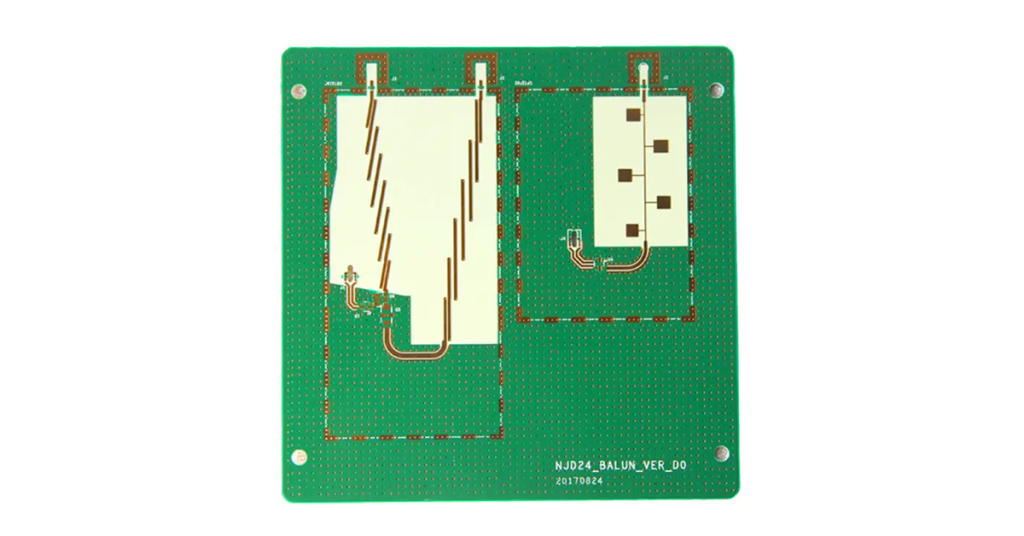
High-Speed High-Frequency PCB Design Guide | Controlled Impedance & RF PCB Layout Techniques Learn advanced high-speed high-frequency PCB design techniques including controlled impedance, low-loss RF materials, stripline routing, back drilling, EMI suppression, and signal integrity optimization for reliable GHz-level performance. high-speed-high-frequency-pcb-design-guide High-Speed High-Frequency PCB Design Guide High-speed high-frequency PCB design has become essential in modern […]
What information is required to design a high-frequency circuit board?
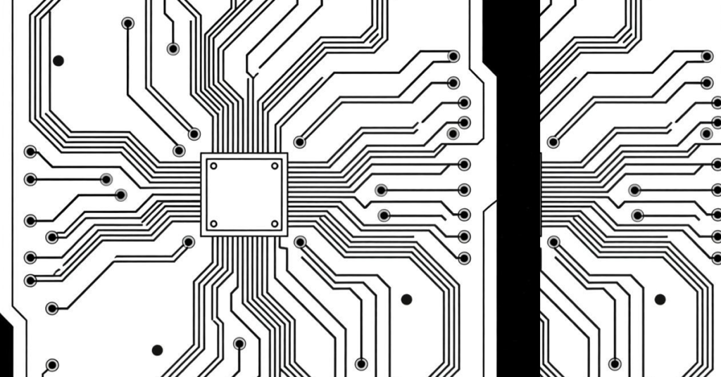
In the world of wireless communication, radar systems, and satellite technology, the quality of your High-Frequency (HF) PCB is the foundation of your system’s performance. High-frequency boards require much tighter tolerances than standard FR-4 boards to maintain signal integrity and minimize dielectric loss. At Shenzhen Xincheng’er Circuit Technology Co., Ltd., we specialize in rapid prototyping […]
High-Frequency PCB Materials and Design Guide for 5G, Radar, and High-Speed Communication Applications

Discover how high-frequency PCBs improve signal integrity in 5G, radar, satellite communication, and high-speed data transmission. Learn about PTFE, Rogers, LCP, impedance control, PCB stackup design, and material selection for RF and microwave applications. https://hfpcbpro.com/high-frequency-pcb/ High-Frequency PCB Materials and Design Guide High-frequency PCB technology plays a critical role in modern wireless communication, radar systems, satellite […]
Key Considerations for High-Frequency PCB Design and Fabrication

Key Considerations for High-Frequency PCB Design and Fabrication I. Design Phase: Focusing on Signal Integrity and Electromagnetic Compatibility II. Fabrication Phase: Precision Processes and Material Adaptation III. Testing Phase: Rigorous Verification of Signal Integrity IV. Golden Rules for High-Frequency PCB Design and Fabrication
Steps and Considerations for Impedance Control in High-Frequency PCB Manufacturing
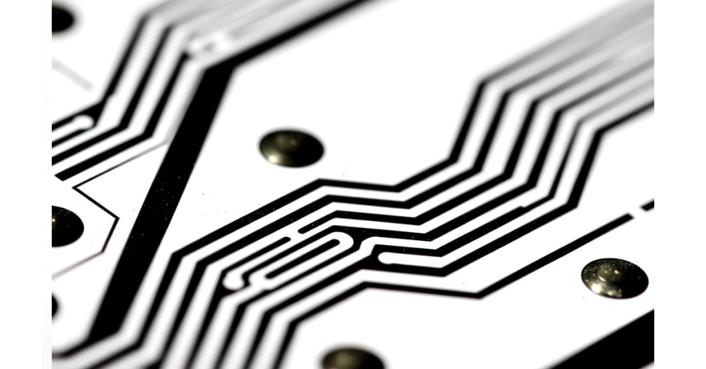
Impedance control is crucial for signal integrity and circuit performance in high-frequency PCBs, especially in applications involving RF, microwave, and high-speed digital signal transmission. Impedance affects signal transmission speed, reflection, distortion, and other factors, making precise impedance design and control critical for ensuring circuit performance. Below are the main steps and considerations for impedance control […]
High-Frequency PCB Production: Steps and Considerations for Microstrip and Stripline Design
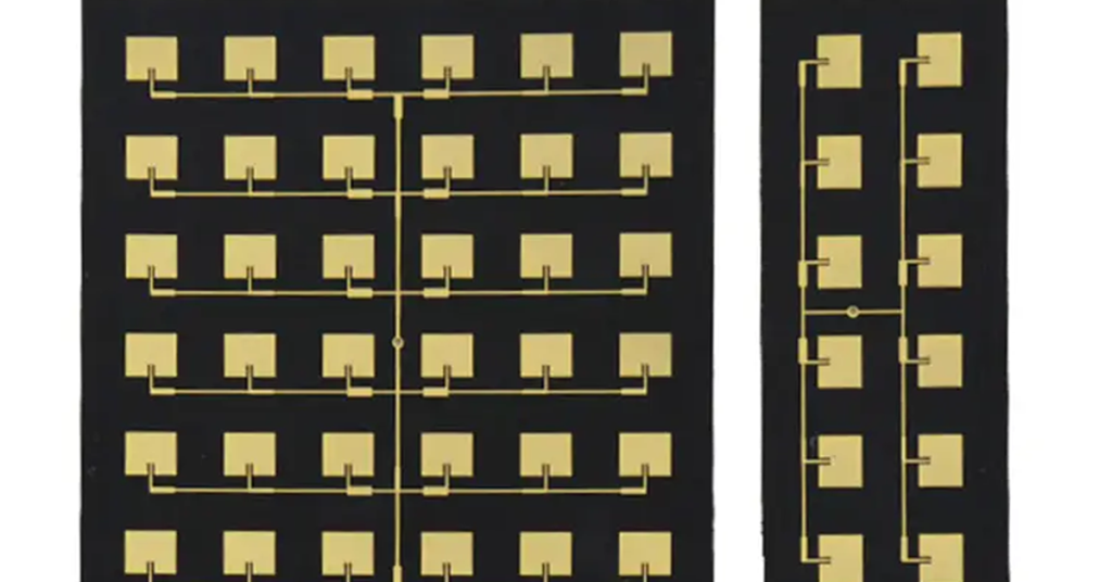
I. Basic Concepts of Microstrip and StriplineMicrostrip: A widely used transmission line structure in high-frequency circuits, typically composed of a metal conductor and an insulating substrate. The characteristic impedance of microstrip is influenced by its width, thickness, and dielectric constant of the substrate.Stripline: Usually consists of two parallel conductors and is commonly used to control […]
PCB manufacturing, route width refers to what, performance and role?
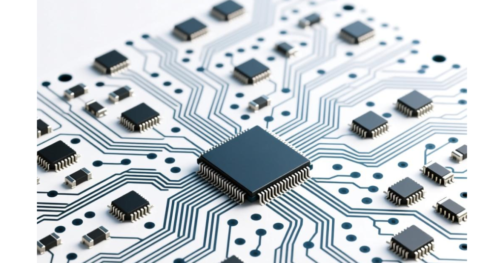
In PCB manufacturing, “trace width” specifically refers to the physical width of copper conductors on a printed circuit board. As a core parameter in PCB design, trace width directly determines the electrical characteristics, thermal management efficiency, signal transmission quality, and production costs of a circuit. The following provides a professional analysis of trace width performance […]
5G Antenna Array PCB Design: 5 Key Technologies for Impedance Consistency Control
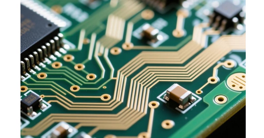
In 5G communication systems, particularly those utilizing massive MIMO and millimeter-wave technologies, antenna array performance directly determines overall system throughput, coverage range, and signal quality. The foundation of these antenna arrays lies in their underlying printed circuit boards. At high-frequency 5G signal rates, PCBs transition from simple connection carriers to integral components of the RF […]
English: How to Design a PCB with Controlled Impedance in High-Frequency Applications
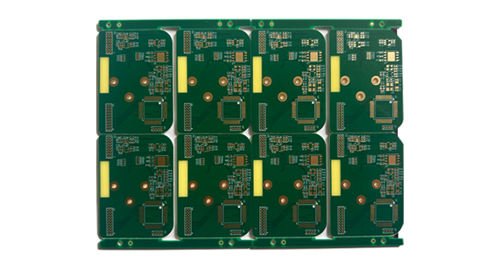
In high-frequency PCB applications, controlled impedance is a critical requirement to ensure signal integrity and reduce signal reflection. Controlled impedance refers to the characteristic impedance of transmission lines being designed to remain consistent within a specific range, typically 50Ω or 75Ω, to meet the needs of high-speed or high-frequency signals. Below is a detailed guide […]
Design Advantages of Blind and Buried Vias in High-Frequency PCBs
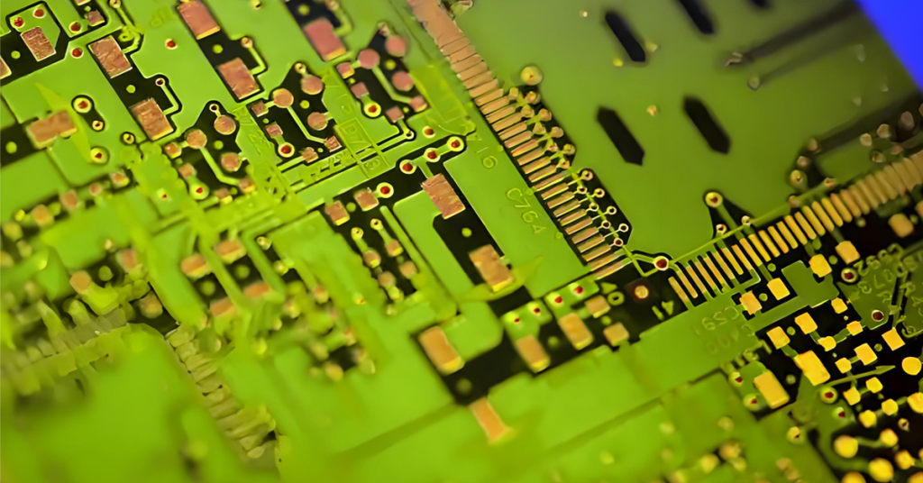
In high-frequency PCB (Printed Circuit Board) design, signal integrity, impedance control, and loss reduction are critical core objectives. Traditional through-hole vias, with their long stubs and significant parasitic effects, often struggle to meet stringent high-frequency requirements. The adoption of blind vias and buried vias offers significant advantages in addressing these challenges. 1. Greatly Enhanced Signal […]