
RO3003 Bond vs RO4450: Differences, Lamination Process, and Best Bonding Material for Rogers RO3003 PCB
RO3003 Bond vs RO4450: Differences, Lamination Process, and Best Bonding Material for Rogers RO3003 PCB ro3003-bond-vs-ro4450 Meta Description Learn why Rogers RO3003 PCB cannot be directly laminated and compare RO3003 Bond with RO4450. Discover differences in material type, lamination process, dielectric properties, manufacturing cost, and the best applications for high-frequency and mmWave PCB designs. RO3003 […]
High-Frequency PCB Surface Finishes Compared: ENIG vs Silver vs Tin for RF and Microwave Applications
Learn how different high-frequency PCB surface finishes impact signal integrity. Compare ENIG, immersion silver, and immersion tin in terms of insertion loss, conductivity, roughness, and RF performance for 5G, radar, and microwave applications. https://www.yourdomain.com/high-frequency-pcb-surface-finishes-enig-vs-silver-vs-tin High-frequency PCB performance depends on much more than substrate selection. While designers often focus on dielectric constant (Dk), dissipation factor (Df), […]
How to solve the problems of compression alignment and expansion/contraction?
High Frequency Multilayer PCB Lamination Alignment and Material Expansion Control for RF & 5G Applications Learn how high frequency multilayer PCB manufacturers solve lamination alignment and material expansion issues in RF, 5G, millimeter-wave, and satellite communication PCBs. Discover advanced registration control, LDI imaging, mixed lamination technology, and dimensional compensation solutions. multilayer-pcb-lamination-registration-contro High Frequency Multilayer PCB […]
FR-4 and RO4250B PCB Lamination Processing Guide: Key Manufacturing Considerations for High-Frequency PCBs
Learn the differences between FR-4 and RO4250B PCB materials, their lamination processing requirements, drilling considerations, reliability testing, and best practices for manufacturing high-frequency PCBs with superior performance and stability. /fr4-ro4250b-pcb-lamination-processing-guide FR-4 and RO4250B PCB Lamination Processing Guide FR-4 and RO4250B PCB lamination processing plays a critical role in determining the performance, reliability, and manufacturability of […]
Important Considerations for the Customization Process of High-Frequency Printed Circuit Boards
Learn the complete high-frequency PCB customization process, from material selection and impedance control to manufacturing, testing, and quality assurance. Discover best practices for RF, microwave, 5G, and radar PCB projects. High-Frequency PCB Customization Guide: From Material Selection to Mass Production High-frequency PCB customization has become increasingly important as industries continue to adopt advanced technologies such […]
ENIG, Plated Gold, DIG, Thick Gold, Thin Gold—What’s the Difference?
Gold Surface Finishes for Hardware, RF, PCB & Microassembly Engineers Gold surface finishes can be extremely confusing:ENIG, plating gold, nickel-gold, immersion gold, thick gold, thin gold, palladium-gold, DIG…One tiny difference in name leads to huge gaps in cost, reliability, high-frequency performance, solderability, and bondability. I will break down every finish clearly:Name → Structure → Process […]
Finished Product Testing and Environmental Simulation Equipment in the Production Process of High-Frequency PCBs
With the rapid development of fields such as high-frequency communication, 5G, satellite navigation, and radar technology, the application of high-frequency PCBs (Printed Circuit Boards) in modern electronic devices is becoming increasingly widespread. High-frequency PCBs require extremely high precision and stability in the transmission of high-frequency signals. Therefore, every step of their manufacturing process requires precise […]
Post-Processing Steps and Considerations in High-Frequency PCB Production
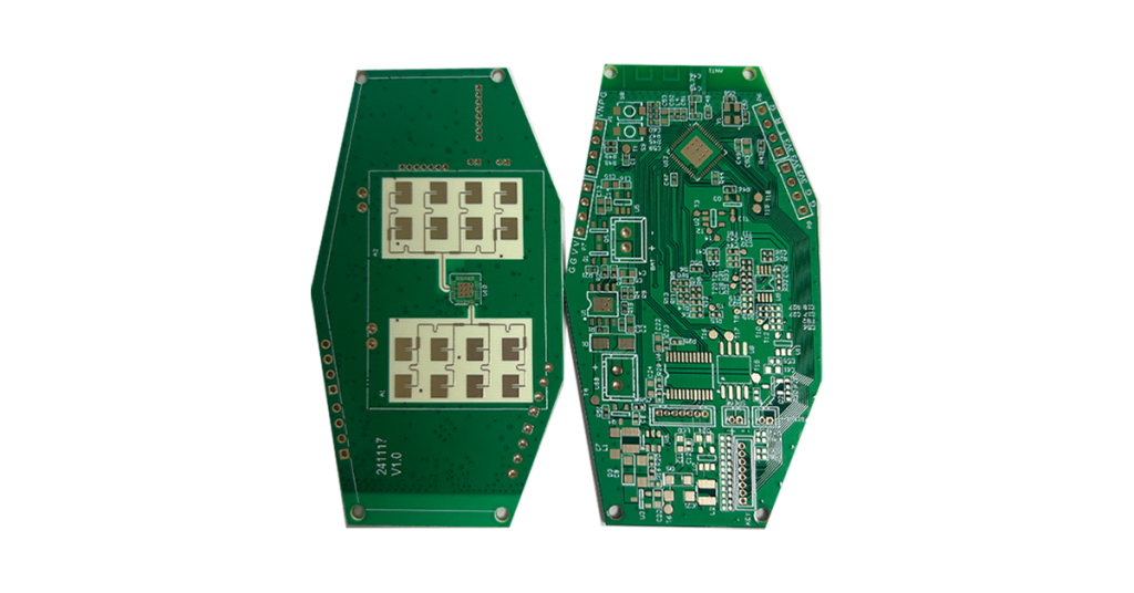
I. Main Post-Processing StepsSurface Cleaning Step: After processes like electroplating, etching, and soldering, high-frequency PCBs may have chemical residues or contaminants. Use ultrasonic cleaning, chemical cleaning, or high-pressure water cleaning to remove these residues and ensure the PCB surface is clean.Consideration: Ensure that the cleaning agent does not damage the PCB surface. Surface smoothness is […]
Steps and Considerations for Surface Treatment in High-Frequency PCB Production
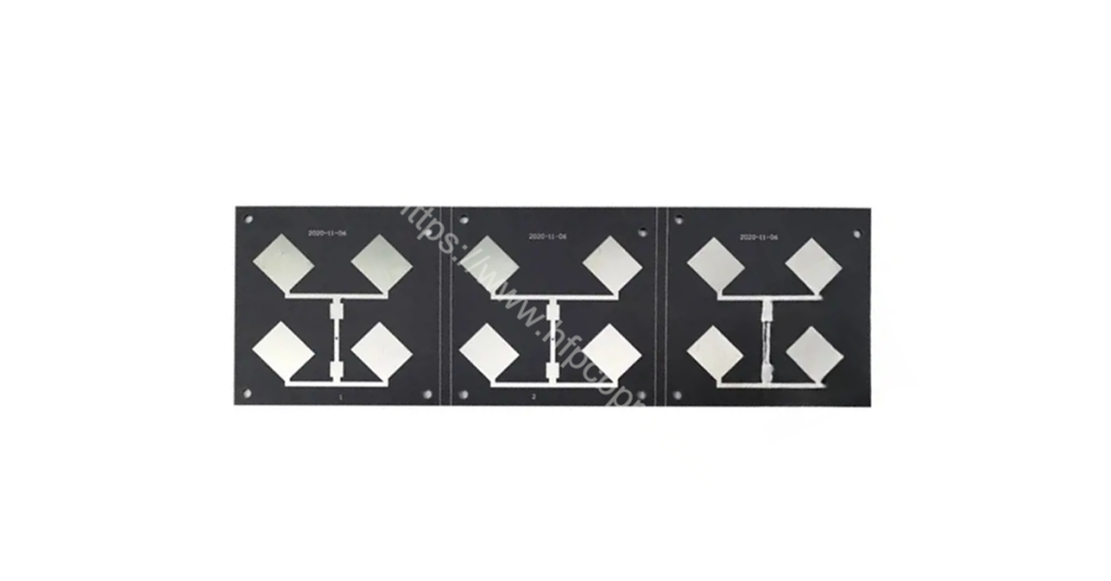
Surface treatment in the production of high-frequency PCBs (Printed Circuit Boards) is a crucial step that directly affects the board’s solderability, corrosion resistance, and electrical performance. Surface treatment typically includes processes such as gold plating, tin plating, immersion gold, and immersion tin. Here are the main steps and considerations for surface treatment in high-frequency PCB […]
Laser Engraving and Marking Equipment in High-Frequency PCB Manufacturing
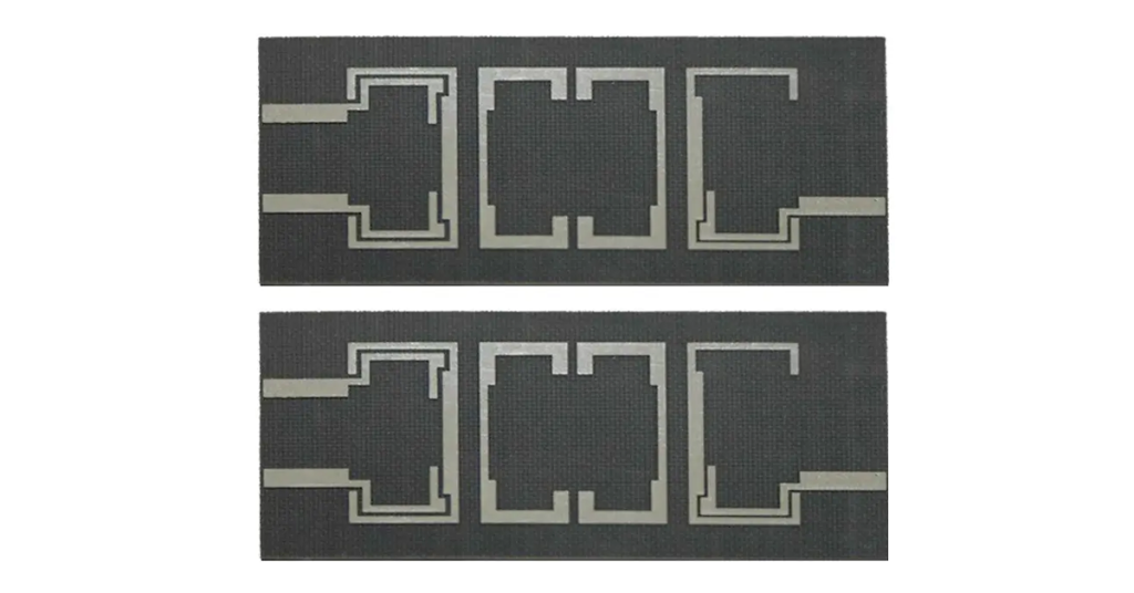
High-frequency PCBs (High-Frequency Printed Circuit Boards) are widely used in fields demanding high precision and stringent requirements, such as communications, radar, satellite navigation, and medical applications. In the production process of high-frequency PCBs, precise engraving and marking are crucial. Laser engraving and marking equipment serves as a vital tool in modern high-frequency PCB processing, offering […]
Optical Microscopes and Electron Microscopes in High-Frequency PCB Manufacturing
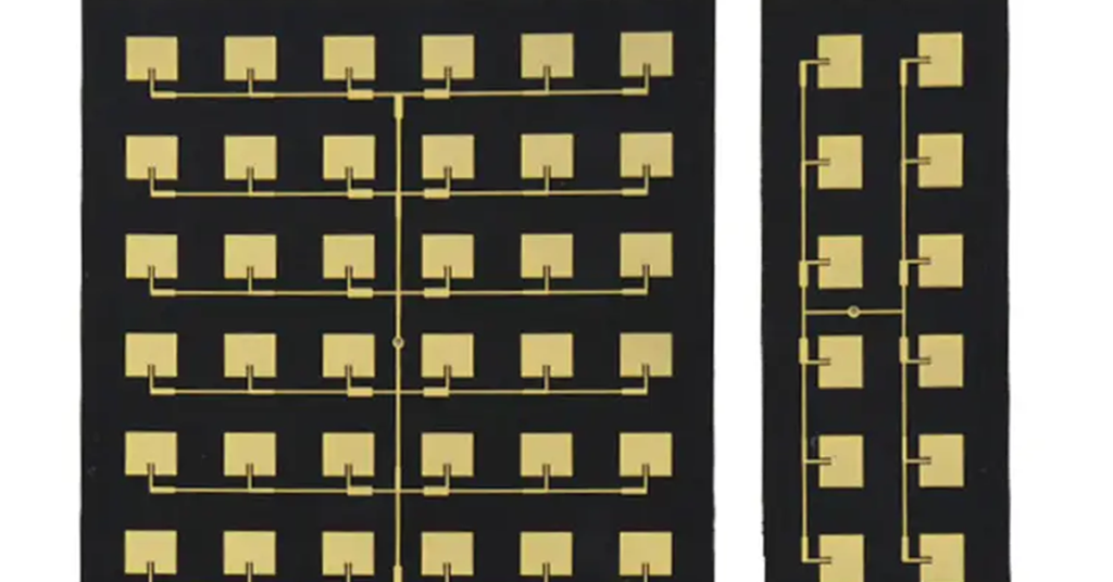
High-frequency PCBs (Printed Circuit Boards) are key components in electronic devices, widely used in fields such as communications, radar, and satellite navigation. With the advancement of high-frequency technology, the complexity and precision of PCB design continue to increase, placing higher demands on their manufacturing processes. In the production of high-frequency PCBs, optical microscopes and electron […]
Laser Etching Machine in High-Frequency PCB Production Process
高频PCB激光蚀刻技术应用概述 请用谷歌收录规则帮我翻译成英文:在高频PCB(高频印刷电路板)的生产过程中,蚀刻工艺是实现电路图案形成的重要步骤。传统的蚀刻方法通常采用化学蚀刻,而激光蚀刻机作为一种先进的蚀刻技术,近年来在高频PCB加工中得到了广泛应用。激光蚀刻机具有高精度、高效率、非接触式等优点,特别适用于高频PCB材料的加工。由于高频PCB对电气性能、信号传输的要求极高,激光蚀刻机在PCB加工过程中能够确保图案的精准性和电气性能,避免传统蚀刻方式中可能出现的误差和不一致性。 本文将详细介绍激光蚀刻机在高频PCB生产中的应用、工作原理、优势以及它在高频PCB工厂中的重要性。 1. 激光蚀刻机概述 激光蚀刻机是一种通过激光束在PCB表面进行精细蚀刻的设备。激光器通过高能激光束将光能聚焦到PCB表面,从而对铜层进行蚀刻,去除不需要的铜部分,形成电路图案。与传统的化学蚀刻方法不同,激光蚀刻机利用光学技术进行非接触式操作,具有非常高的精度和效率,尤其适合用于高频PCB的生产。 在高频PCB的生产过程中,激光蚀刻机能够处理多种特殊材料,如PTFE(聚四氟乙烯)、陶瓷、聚酰亚胺等,这些材料通常具有较高的强度和特殊的电气性能。激光蚀刻技术能够在保证电气性能的同时,确保加工精度,避免因过度腐蚀或图案模糊导致的信号损失。 2. 激光蚀刻机的工作原理 激光蚀刻机的工作原理基于激光的热效应,利用激光束在材料表面聚焦释放出能量,从而达到蚀刻铜层的效果。具体过程如下: 2.1 激光束产生与聚焦 激光蚀刻机通过激光器产生高能量的激光束,并通过镜头系统将激光束聚焦到一个非常小的点上。这个点的光能集中,使材料表面产生高温,导致材料的蒸发或熔化。 2.2 精确控制与扫描 激光蚀刻机利用计算机控制系统精确控制激光束的位置、移动轨迹和扫描速度。激光束在PCB的表面按照设计文件的路径进行扫描,将不需要的铜层去除,最终形成电路图案。计算机控制系统根据预设的设计图案,控制激光束的扫描路径,确保图案的精度和质量。 2.3 去除铜层 激光束在照射到PCB表面时,会将铜层局部加热到熔点并进行蒸发或熔化,去除不需要的铜部分,留下所需的电路图案。这一过程无需接触材料,因此避免了传统化学蚀刻中可能发生的机械应力损伤。 2.4 冷却与清洗 蚀刻完成后,PCB表面会被冷却和清洗,去除残留的杂质和材料,确保表面干净,避免任何影响后续工艺的因素。 3. 激光蚀刻机在高频PCB生产中的应用 激光蚀刻机在高频PCB的生产中具有多方面的应用,特别是对于高频电路板的精密加工,它提供了传统方法无法比拟的精度和效率。 3.1 高精度电路图案转移 高频PCB的电路图案通常非常复杂,尤其是高频信号路径的设计,要求非常高的精度和稳定性。激光蚀刻机能够通过计算机精确控制激光的路径,确保每个电路的宽度、间距和形状都符合设计要求。高精度的电路图案转移,保证了电路的信号传输性能和稳定性。 3.2 微小孔径和细线条加工 随着PCB设计的微型化,越来越多的高频PCB需要处理微小的孔径和细线条。激光蚀刻机能够精确加工这些微小孔径和细线条,确保高密度布线和复杂图案的加工。这对于高频PCB中微型元器件的焊接以及微小连接的电气性能尤为重要。 3.3 多层PCB的蚀刻 高频PCB通常采用多层结构,并且不同层之间有许多连接孔。激光蚀刻机能够精准地加工每一层电路,确保多层之间的连接孔位置准确,且各层之间的信号传输不受影响。此外,激光蚀刻技术的精度能够满足多层PCB的高密度布线需求,确保信号不发生损失。 3.4 特殊材料的蚀刻加工 高频PCB常用的材料,如PTFE(聚四氟乙烯)、陶瓷和聚酰亚胺等,具有较高的强度和特殊的电气特性,传统的蚀刻方法可能无法有效加工这些材料。激光蚀刻机能够处理这些特殊材料,确保高频PCB在这些材料上的精确图案形成,避免传统化学蚀刻方法对材料造成的损伤或误差。 3.5 提高生产效率 激光蚀刻机与传统的化学蚀刻方法相比,能够显著提高生产效率。激光蚀刻是非接触式加工,无需复杂的化学处理步骤,能够在较短时间内完成高精度的电路图案加工。对于大批量生产的高频PCB,激光蚀刻机能够大幅度提高生产速度,并降低生产成本。 4. 激光蚀刻机的优势 4.1 高精度与高分辨率 激光蚀刻机能够提供极高的精度和分辨率,通常可以达到微米级别的精度。这对于高频PCB的制造至关重要,因为任何微小的电路图案误差都可能影响信号传输的稳定性和性能。 4.2 非接触式加工 激光蚀刻机通过激光束进行非接触式加工,不会对PCB材料造成任何机械压力或损伤。相比传统的机械蚀刻,激光蚀刻能够避免因材料变形或损坏而导致的电气性能问题。 4.3 适应复杂设计 激光蚀刻机能够处理各种复杂的电路设计,包括高密度线路、微小孔径和复杂图案。对于现代高频PCB的复杂设计,激光蚀刻机能够灵活适应,并确保每个细节的精准加工。 4.4 高效生产 激光蚀刻机的加工速度较快,能够大幅度提高生产效率,适应大规模的PCB生产。激光束能够快速扫描并处理大面积的电路图案,缩短生产周期,满足快速交货的需求。 4.5 […]