High-frequency multilayer PCBs carry GHz-level signals in 5G base stations, automotive radar, satellite payloads and aerospace electronics. Compared with a standard FR-4 board, nothing about the process is forgiving: Dk has to stay stable, Df has to stay low, impedances have to hold at 50Ω or 75Ω, and every layer has to land where it should. From what we see on the production floor, over 80% of RF PCB failures trace back to material mismatch and lamination instability — not to circuit design. This guide walks through the whole manufacturing process and the control points that decide whether a high-frequency board actually performs.
Everything starts with the substrate. A laminate that looks fine on a datasheet can still cause trouble in lamination or drilling, so material choice is a manufacturing decision as much as an electrical one.
The materials we run most often on high-frequency builds:
Each of these behaves differently under heat and pressure, which is why the stack-up has to be planned around the material — not the other way round.
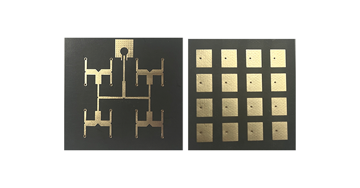
A good RF stack-up keeps every signal layer next to a continuous reference plane and uses a symmetrical build to resist warpage. Mixing materials needs care: when PTFE sits next to FR-4, the difference in thermal expansion shows up later as delamination — usually after assembly, when it costs the most.
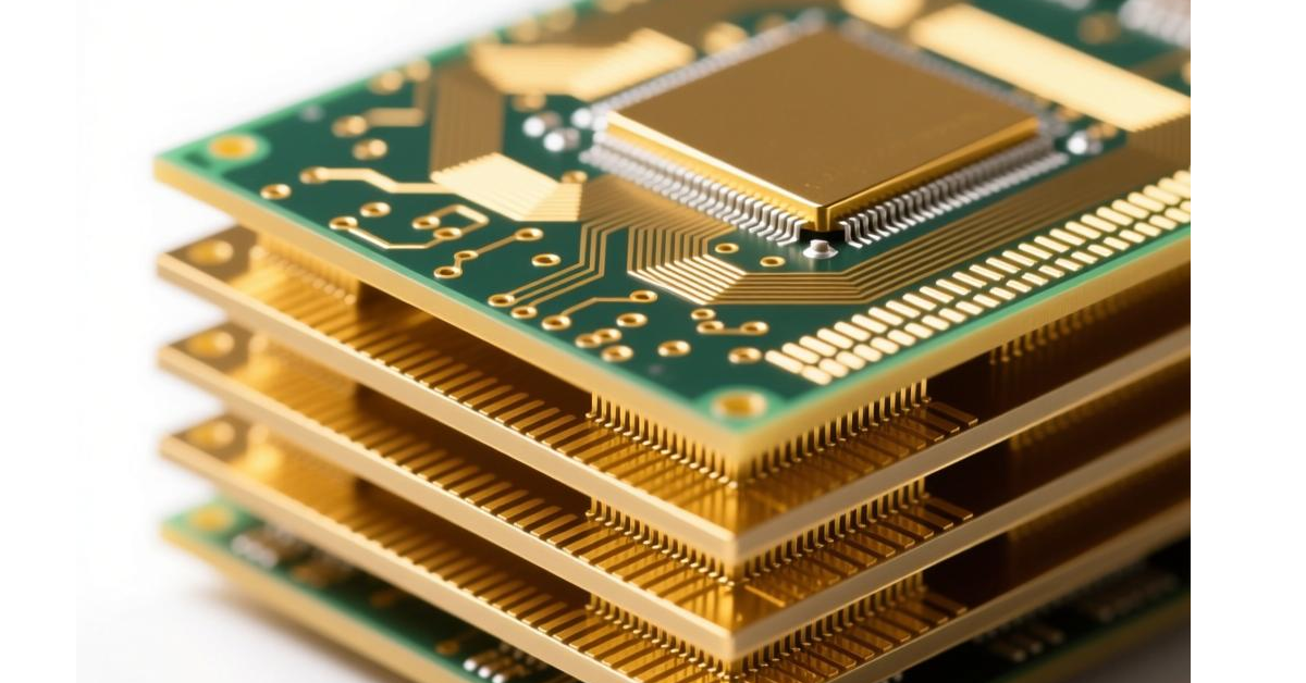
Lamination is where most high-frequency boards are won or lost. PTFE-based stacks go through vacuum lamination rather than a standard press cycle:
Two failure modes come up again and again:
Because PTFE moves more than FR-4 during lamination, alignment has to be calculated, not assumed. We model material shrinkage before production, laminate with a pin system, and correct for thermal expansion across the cycle. The target is layer-to-layer registration within ±25 μm.
PTFE and Rogers laminates are mechanically soft and thermally sensitive — the exact opposite of what a drill bit likes. A hole can look clean and still have smeared resin on the wall, which destroys plating adhesion downstream.
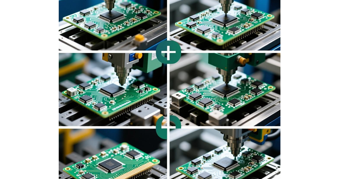
Drill parameters have to be tuned per material — feeds and speeds that work fine on FR-4 will tear up a PTFE hole wall.
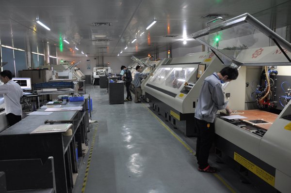
Via metallization decides how well a hole survives thermal cycling. We plate on a VCP (Vertical Continuous Plating) line and use pulse plating to keep copper deposition even from knee to knee.
Electrical test alone can’t tell you how a via was actually plated. That’s what cross-sections are for — we mount, polish and inspect real coupons cut from the production panel.
High-frequency PCB performance is decided more by manufacturing consistency than by circuit design complexity.
Production data keeps pointing to the same three factors:
If you’re planning a high-frequency build, these pages cover the wider context:
A high-frequency multilayer PCB is a precision system. Low-loss transmission, stable impedance and electromagnetic compatibility at GHz frequencies all come down to the same few process steps being done right, board after board. Get the material system, the lamination and the impedance control right, and the finished board will hold up in 5G infrastructure, automotive radar, satellite communication and aerospace electronics — places where rework isn’t an option.
Common questions about high-frequency multilayer PCB manufacturing — for project-specific review, contact our team directly.
A multilayer board built on low-loss materials — Rogers, PTFE, Taconic and similar laminates — engineered to carry GHz-level signals with stable impedance and minimal dielectric loss. Typical uses are 5G, automotive radar and satellite systems.
FR-4's dielectric loss climbs sharply above a few GHz, and its Dk drifts with temperature. Rogers laminates keep loss low and impedance stable at high frequencies — which is what actually matters once you're designing for 5G or radar bands.
Lamination. It determines layer alignment, interface quality and long-term delamination risk — and most of the RF failures we analyze trace back to it.
A hyper very low profile copper foil with an extremely smooth surface. At high frequencies current only travels through the outer skin of the conductor, so foil roughness adds real loss — HVLP foil keeps that conductor loss down.
5G communication, automotive radar, satellite communication, aerospace electronics and high-speed networking.
Send us your stack-up, laminate and frequency band. Our engineers will review material compatibility, lamination feasibility and impedance control, then quote your RF PCB.
Get An RF PCB Quote → Fast Reply on WhatsApp