Stackup decisions sit upstream of everything: signal integrity, EMC, impedance control, power distribution. Yet a lot of designers pour their energy into routing, component placement and decoupling capacitors, and treat the stackup as a detail to settle later. That’s backwards — a poor stackup can turn an otherwise working design into an EMI nightmare.
Consider an illustrative redesign in which a six-layer board is reduced to four layers. If a power or reference plane is fragmented, high-speed return currents may take longer paths, increasing loop area and radiated emissions. An emissions peak near 72 MHz and an 8 dB compliance margin would require actual laboratory measurements to substantiate; these figures should not be treated as a documented customer test result.
A stackup influences three performance areas, and weakness in any one of them shows up in the finished product:
Every high-speed signal needs a nearby reference plane to give its return current a predictable path. Get that right and you:
The spacing between signal layers and their reference planes directly controls radiated emissions. Tighter spacing means:
Plane capacitance comes from the spacing between power and ground planes. More capacitance buys you:
Fall short in any of these areas and the whole board pays for it.
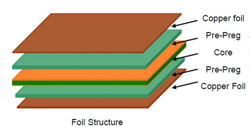
TOP → GND → POWER → BOTTOM
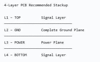
TOP (signal) → GND (solid reference) → POWER (ideally continuous where used as a reference) → BOTTOM (signal)
| Layer | Function |
|---|---|
| TOP | Signal routing |
| GND | Solid ground plane |
| POWER | Power plane |
| BOTTOM | Signal routing |
Good top-layer return paths when L2 is continuous; straightforward construction; cost-effective for many applications. Bottom-layer high-speed signals need particular attention because their nearest reference is often L3, which may be split into voltage islands.
Keep L2 ground continuous. Do not route critical bottom-layer signals across gaps or splits in L3 without providing a suitable continuous return reference. Where bottom-layer routing is critical, consider an alternative stackup with two ground reference planes and distribute power with traces or pours as appropriate.
This variant makes sense when:
The trade-off is power integrity: a mixed signal/power layer usually loses reference-plane continuity.
Some designers use this to gain routing resources, but it creates real problems:
For modern high-speed digital or RF work, don’t.
A six-layer stackup can provide additional routing capacity and well-controlled reference planes, but the benefit depends on the actual layer order, dielectric spacing and reference-plane continuity. Place critical signals adjacent to uninterrupted planes; a signal layer between two reference planes can form a stripline structure.
The inner signal layer sits between two reference planes — a stripline structure that cuts radiated EMI dramatically.
More routing space, less reference-plane integrity. It suits:
Expect to spend extra time on spacing and crosstalk analysis.
Six-layer fabrication typically costs more than four-layer fabrication because of additional cores or foil, prepreg, imaging and etching, registration, drilling considerations, materials and sometimes lamination complexity. The exact increase depends on the construction and fabrication process; an extra lamination cycle is not automatically required for every six-layer board.
Compare total system cost, not just bare-board price. A suitable six-layer design may reduce routing congestion, EMI mitigation work or redesign risk, but savings are project-specific and should be checked with a manufacturer quotation.
The go-to stackup for:
Closely spaced power and ground planes can add useful distributed capacitance, but this depends on their overlap area and dielectric separation. It does not eliminate the need for appropriate decoupling capacitors and PDN analysis.
Thickness is the other half of the stackup decision:
Advantages: common connector compatibility, mechanical rigidity and broad manufacturing availability. The total board thickness alone does not determine plane spacing, capacitance or power integrity; the internal dielectric construction does.
Trade-offs: thicker overall boards can constrain some compact products, but PDN performance must be assessed from the actual power-ground plane spacing and decoupling network.
Increasingly common in embedded and consumer products.
Potential advantages: reduced weight and profile, and suitability for some compact assemblies. Power integrity and solder-joint reliability depend on the full stackup, component package, support conditions and assembly design rather than thickness alone.
Trade-off: reduced bending stiffness may require additional mechanical support or careful assembly handling.
Used in selected compact, RF and HDI applications where mechanical and electrical requirements permit; 0.8 mm is not a universal RF board thickness.
Potential advantages: reduced weight and thickness, and flexibility for compact constructions. Controlled impedance and high-frequency performance still depend on dielectric spacing, Dk, copper thickness and transmission-line geometry.
Trade-offs: lower stiffness, possible connector constraints and additional assembly support requirements.
The stackup determines the dielectric thickness and reference planes available for controlled-impedance traces. A 50 Ω microstrip width cannot be determined from overall board thickness alone: it depends on distance to the reference plane, dielectric constant, finished copper thickness, solder mask and trace geometry. For example, an 8 mil or 4 mil trace might meet 50 Ω in a particular construction, but neither value is a universal rule for a 1.6 mm or thinner PCB. Confirm widths using a field solver and the fabricator’s actual stackup before finalizing BGA breakout and routing.
The stackup is the foundation everything else sits on — signal integrity, EMC compliance, power integrity. Whether it’s a simple four-layer controller board or an eight-layer FPGA platform, getting the layer arrangement right early removes risk from the whole project. Structure, dielectric thickness, plane spacing and impedance targets deserve real decisions at the start of the design, not at the end.
Common questions about PCB stackup design — for project-specific review, contact our team directly.
TOP–GND–POWER–BOTTOM. It gives top-layer routing a solid ground reference, it's cheap to fabricate, and EMI performance is good as long as the ground plane stays continuous.
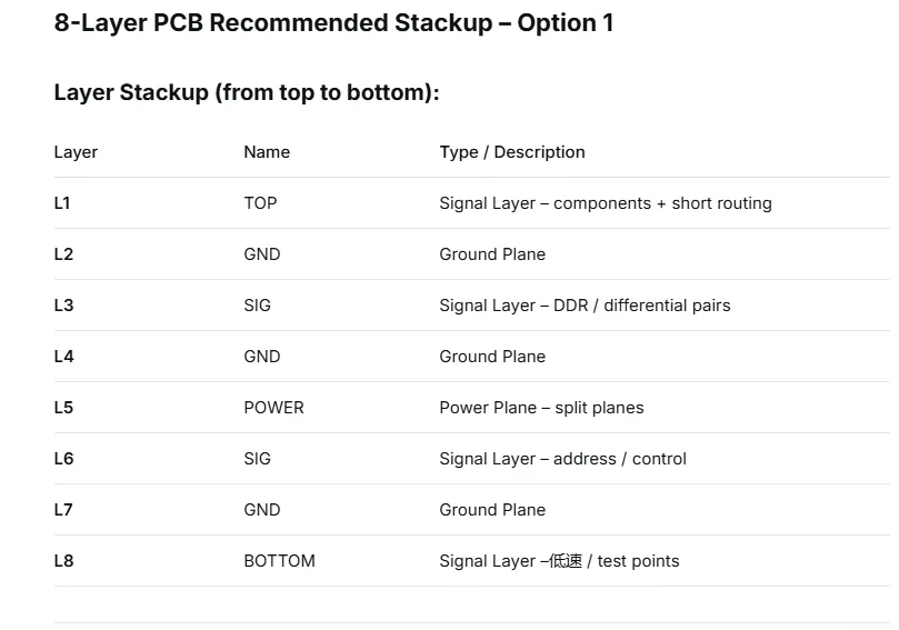
Two dedicated ground planes and an internal stripline signal layer. That means shorter return paths, lower EMI, tighter impedance control and better power distribution — and the difference shows up clearly in EMC testing.
When the design carries real high-speed traffic: FPGA banks, DDR4/DDR5, PCIe, SerDes and networking. Every signal layer gets its own reference plane, and the power–ground pair adds plane capacitance for free.
Yes. Thickness sets the dielectric spacing, and dielectric spacing sets the trace width needed to hit a target impedance — the same 50Ω can mean an 8 mil trace on 1.6 mm or roughly 4 mil on a thinner stack.
Breaking up the reference planes. Fragmented ground or power planes force return currents into long detours, and the resulting loops radiate — that's how a board that simulates fine fails EMC on the bench.
Send us your layer count, target impedance and key interfaces. Our engineering team will review the stackup, check manufacturability and quote your multilayer PCB.
Get A Stackup Review → Fast Reply on WhatsApp