PCB Stack-Up Design Guide: How High-Speed and High-Frequency PCBs Ensure Performance from the Structure
PCB stack-up design coordinates conductive and dielectric layers to support controlled impedance, predictable return paths, power distribution, and practical PCB fabrication. This guide focuses on design principles and includes a real six-layer Rogers RO4350B stack-up example.
Table of Contents
What Is PCB Stack-Up?
A PCB stack-up defines the order and construction of conductive and dielectric layers. For high-speed and RF designs, the layer arrangement influences reference planes, impedance control, signal coupling, and manufacturability. The following sections explain practical stack-up design principles and present a customer-supplied six-layer Rogers PCB fabrication example.
Why Does Stack-Up Design Affect Signal Integrity?
Impedance, Return Path, and EMI
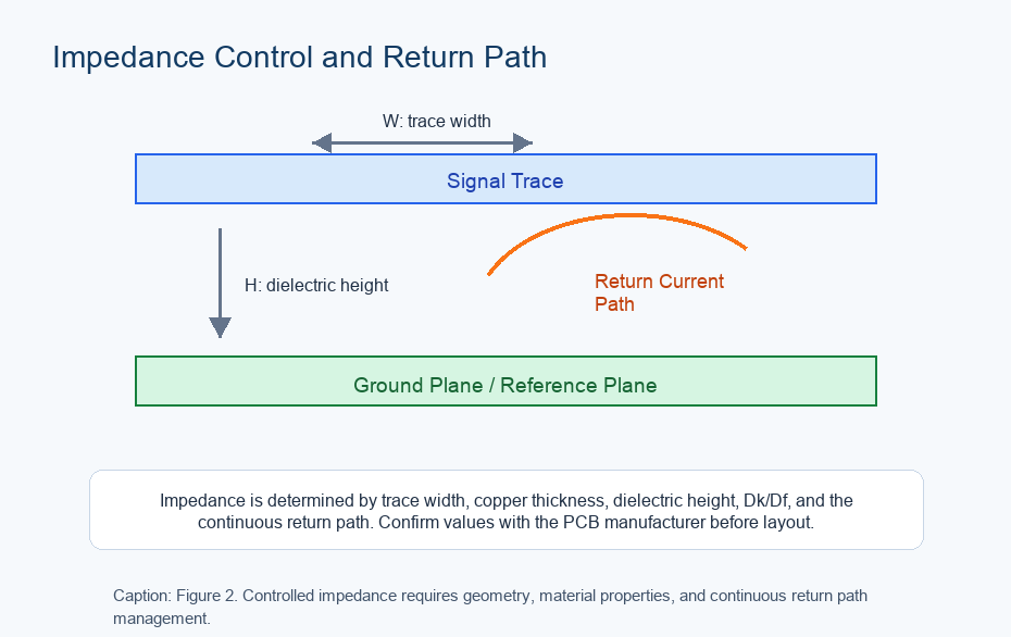
At high frequencies, return current tends to concentrate near the signal trace on a continuous reference conductor. Its distribution depends on the transmission-line geometry and surrounding conductors. Crossing a reference-plane split can increase return-path inductance, common-mode conversion, crosstalk, and radiated emissions. Signal reflections depend on the resulting impedance discontinuity.
Impedance control depends not only on trace width, but also on copper thickness, dielectric thickness, Dk/Df, surface copper roughness, and the actual thickness after lamination. Therefore, designers should provide target impedance values and tolerances, while the manufacturer verifies them through material selection and TDR testing.
Key Rules for High-Speed and High-Frequency PCB Stack-Up
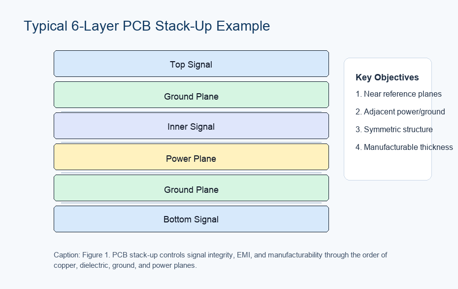
– Place high-speed or RF signal layers next to solid ground planes to reduce loop area and EMI.
– Avoid stacking adjacent signal layers directly together; use orthogonal routing or add ground plane isolation when necessary.
– Keep power and ground planes close together to create a low-impedance PDN, combined with proper decoupling capacitors.
– Maintain stack-up symmetry and balanced copper distribution to reduce warpage and board deformation.
– For HDI designs, control lamination cycles and select blind vias, buried vias, stacked vias, or staggered vias properly.
– For rigid-flex PCBs, choose flexible-layer placement according to the bend direction, required bend radius, layer construction, and fabrication capability. Keep vias and rigid components outside the specified bending zone.
– For high-frequency hybrid stack-ups, pay attention to material CTE, Dk/Df, and lamination compatibility.
Manufacturing Case Study: Six-Layer Rogers RO4350B PCB Stack-Up
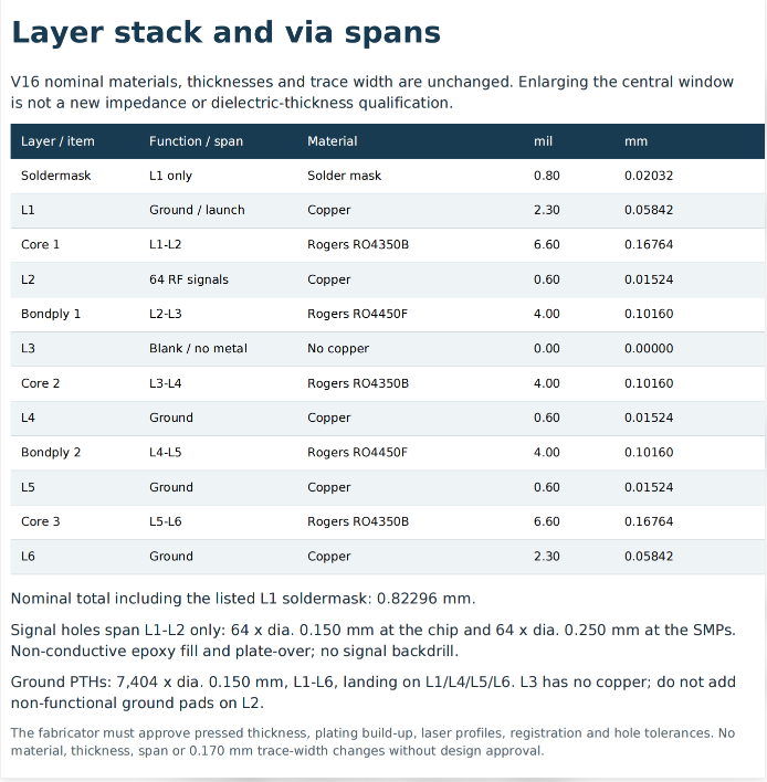
The following customer-supplied fabrication drawing illustrates a specific six-layer RF PCB using Rogers RO4350B cores and RO4450F bondply. It is a design-specific reference, not a universal stack-up recommendation. Nominal material thicknesses and trace widths are unchanged; enlarging the central window does not constitute a new impedance or dielectric-thickness qualification.
The drawing specifies RO4350B core thicknesses of 6.60 mil (L1–L2), 4.00 mil (L3–L4), and 6.60 mil (L5–L6), separated by two 4.00 mil RO4450F bondply layers. L2 carries 64 RF signals; L3 is intentionally blank with no copper. L1 is a ground/launch layer, and L4, L5, and L6 are ground layers. Copper is listed as 2.30 mil at L1 and L6 and 0.60 mil at L2, L4 and L5. The listed L1 soldermask is 0.80 mil. The drawing states a nominal total of 0.82296 mm including that soldermask; this is a drawing sum, not an independently verified finished-board thickness or tolerance.
Signal Vias and Ground Through-Holes
Signal holes span L1–L2 only: 64 × 0.150 mm diameter at the chip and 64 × 0.250 mm diameter at the SMPs, with non-conductive epoxy fill and plate-over; no signal backdrill is specified. Ground plated through-holes are listed as 7,404 × 0.150 mm diameter, spanning L1–L6 and landing on L1/L4/L5/L6. Because L3 has no copper, do not add non-functional ground pads on L2.
Fabrication and DFM Review
The fabricator must approve the pressed thickness, plating build-up, laser-drilling profiles, layer registration, and hole tolerances before production. The drawing specifies that material, thickness, via spans, and the 0.170 mm trace width must not be changed without design approval. Confirm the final stack-up, impedance, manufacturability, and test requirements against the customer’s controlled fabrication files.
What Must Be Clearly Defined in DFM Files?
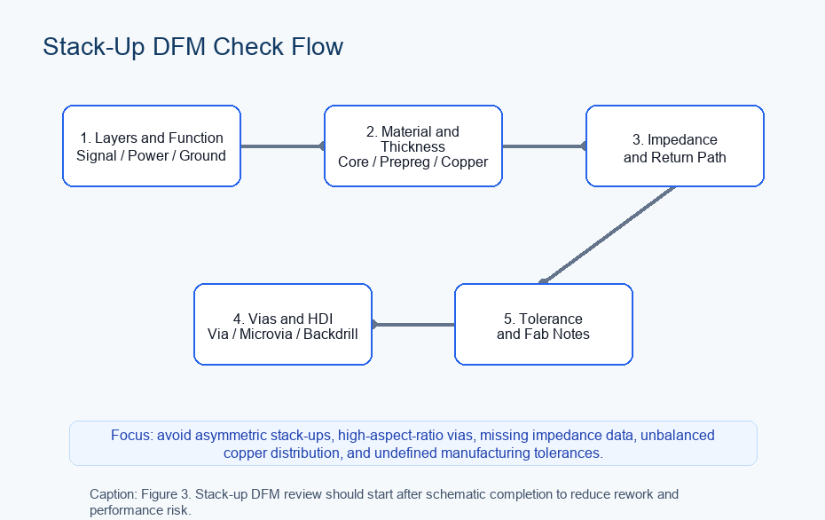
Manufacturing drawings should clearly specify layer sequence, material model, core/prepreg thickness, copper thickness, total board thickness and tolerance, impedance trace locations, dielectric constant, dissipation factor, surface finish, solder mask color, via structure, IPC class, and testing requirements.
Missing impedance data, high-aspect-ratio vias, unbalanced copper distribution, or asymmetric stack-up can increase the risk of rework, warpage, and performance failure.
Conclusion
An excellent PCB stack-up design is essentially a balance between electrical performance, mechanical reliability, and manufacturing capability. For high-speed, high-frequency, HDI, rigid-flex, and hybrid PCBs, confirming the stack-up, impedance, and materials as early as possible helps reduce EMI, crosstalk, lamination risk, and mass production cost.
Frequently Asked Questions About PCB Stack-Up Design
Quick answers from HF PCB PRO engineering — for project-specific stack-up review, contact our team directly.
How many layers does a high-speed or high-frequency PCB stack-up need?
There is no fixed number. Simple RF boards often work on 2–4 layers, while high-speed digital, HDI and backplane designs commonly use 6–12 or more. What matters is not the count but the discipline: every high-speed or RF signal layer should face a solid, unbroken reference plane, and power and ground planes should be closely paired to form a low-impedance PDN.
Should signal layers be placed next to ground planes or power planes?
Ground planes are preferred. High-speed return current flows along the nearest reference plane, so a signal layer adjacent to a solid ground plane gives the shortest return path and the lowest EMI. A power plane can act as a reference only if it is continuous and tightly coupled to a nearby ground plane; signals crossing split or distant power planes are a common source of crosstalk and radiation.
What dielectric thickness and materials are typical for impedance-controlled stack-ups?
Between a surface microstrip and its reference plane, prepreg thickness of roughly 2–8 mil (50–200 µm) is common, with core thickness chosen per the total board thickness and impedance targets. What decides performance is the combination of dielectric thickness, copper roughness and Dk/Df of the laminate. Always state target impedance values and tolerances in the fab drawing, and let the manufacturer verify them by TDR on a coupon.
Can I mix Rogers and FR-4 in one stack-up?
Yes — hybrid stack-ups that laminate low-loss PTFE or hydrocarbon RF layers together with FR-4 digital and power layers are widely used to balance performance and cost. Pay attention to CTE mismatch, lamination compatibility and press cycle control, and keep the flexible definition clear for rigid-flex builds. Your manufacturer should confirm the hybrid layup before fabrication.
Does an asymmetric stack-up really cause manufacturing problems?
It can. Unequal dielectric spacing or unbalanced copper distribution above and below the neutral axis creates uneven stress during lamination and thermal cycling, which leads to warpage and registration drift — especially on thick, high-layer-count or heavy-copper boards. Keep the stack-up symmetric and balance copper area across layers whenever the design allows.
Need Your Stack-Up Reviewed Before Fabrication?
Send us your stack-up drawing or Gerber files — our engineers will check layer sequence, impedance targets, material selection and DFM risks, and reply with a free review and quote.