Selecting the right PCB material for an RF or microwave design is one of those decisions that shows up in every measurement afterwards. High-frequency circuits leave little margin — signal loss, phase drift and unstable electrical properties all trace back to the laminate. The six tips below cover the properties worth checking before you commit.
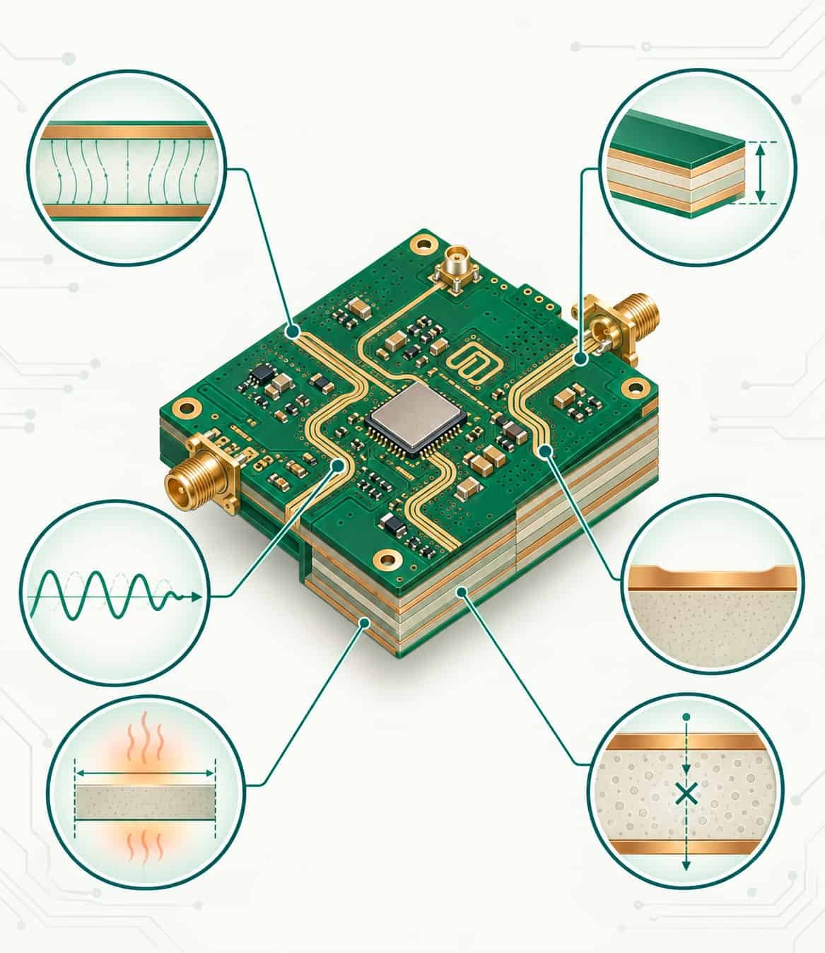
Dielectric constant (Dk) influences transmission-line impedance, phase velocity and the dimensions of RF structures. A lower Dk can help with wider traces and faster propagation, but it is not automatically the best choice: higher-Dk laminates can be useful for compact filters and antennas. Compare design Dk at the relevant frequency, its tolerance and its stability with temperature and moisture.
Variations in Dk can change electrical length, phase and impedance. Check the manufacturer’s test method and distinguish process Dk from design Dk when available. For material examples and specifications, see our RT5870 and RT5880 laminate guide.
Dissipation factor (Df, or loss tangent) describes dielectric energy dissipation. Lower Df generally reduces dielectric insertion loss, but there is no universal Df < 0.005 cutoff for every RF board. Select a laminate based on operating frequency, trace length, allowable insertion loss, temperature and cost. Compare published Df values at comparable test frequencies.
At microwave frequencies, dielectric loss becomes increasingly important, particularly on long transmission lines. However, total insertion loss also includes conductor roughness, geometry, connectors and transitions. A low-Df substrate alone does not guarantee a low-loss assembly.
Thermal performance requires more than one fixed CTE or conductivity target. Review in-plane and Z-axis coefficient of thermal expansion (CTE), glass transition behavior where applicable, thermal conductivity, operating temperature and plated-through-hole reliability. Suitable limits depend on the laminate system, board thickness, via construction and thermal cycling profile; 10–20 ppm/°C is not a universal Z-axis requirement.
CTE mismatch between the dielectric, copper and plated holes can increase mechanical stress during assembly and service. Thermal conductivity matters especially near power amplifiers and other heat sources. Evaluate these properties together with the complete stack-up and the manufacturer’s fabrication recommendations.
Substrate thickness affects microstrip width, field distribution, impedance, coupling, radiation and fabrication tolerances. There is no universal rule that designs above 10 GHz must use 10–20 mil laminates. Determine thickness with an electromagnetic or impedance model using the selected Dk, copper thickness, surface finish and transmission-line geometry.
A thinner dielectric may support compact structures and help control unwanted radiation in some layouts, but it can require narrow traces and increase conductor-loss sensitivity. A thicker dielectric can improve trace width while changing coupling and radiation behavior. Confirm the stack-up with your PCB manufacturer before releasing Gerber files. See our RF PCB material selection guide for related considerations.
At high frequency, current concentrates near conductor surfaces because of the skin effect. Copper surface roughness can add conductor loss, so low-profile foils such as VLP or HVLP may help reduce insertion loss. The best choice also depends on copper thickness, trace geometry, adhesion requirements and the laminate’s available copper-clad constructions.
Do not assume every HVLP foil has better adhesion or that all RO3000 laminates use the same foil. Ask for the actual copper treatment and roughness specifications supplied with the laminate. Copper roughness models are particularly useful when predicting loss at microwave and millimeter-wave frequencies.
Volume resistivity measures a dielectric’s resistance to DC leakage through its bulk. It matters for insulation reliability, particularly under high humidity, elevated temperature or high bias. It should not be treated as the primary predictor of microwave signal leakage, which is more directly influenced by transmission-line fields, Dk, Df, shielding and layout.
For insulation reliability, also examine surface resistivity, moisture absorption and environmental testing. For RF isolation and insertion loss, prioritize the appropriate electromagnetic properties and board geometry rather than relying on volume resistivity alone.
RF PCB material selection is a trade-off among dielectric stability, dielectric and conductor loss, thermal reliability, substrate geometry and fabrication capability. For example, Rogers RO4350B can be attractive where processing convenience matters, while PTFE-based RT5880 may suit designs with more demanding dielectric-loss targets. Confirm the actual laminate grade, copper construction and design frequency against current manufacturer data before ordering.
Official technical resources: Rogers Corporation and Isola Group.
Quick answers from HF PCB PRO engineering — for project-specific advice, contact our team directly.
Below 4 at your operating frequency is the usual target for RF and microwave work; millimeter-wave designs often go lower. Dk consistency across frequency matters as much as the absolute value, because shifts cause dispersion and phase error. Always quote Dk at the design frequency, not at 1 MHz.
Df is the fraction of signal energy converted to heat. At GHz frequencies even small Df differences compound into noticeable insertion loss across a board. Below 0.005 keeps attenuation manageable; PTFE laminates typically reach 0.001–0.003.
Below roughly 1 GHz, sometimes. Above that, FR-4's higher Df (around 0.02), unstable Dk and high Z-axis CTE cost you loss, phase stability and reliability. For anything beyond a few GHz, a low-loss laminate is the safer call.
VLP, HVLP and RTF foils have smoother surfaces than standard electrodeposited copper. Above a few GHz, where current crowds toward the conductor surface, roughness drives conductor loss. Low-profile foil cuts that loss, at some cost in adhesion.
Typically 10–20 mil. Thin substrates shorten the signal path, reduce dielectric loss and tighten impedance control. Very thin laminates trade away mechanical strength, so confirm handling and rigidity requirements with your fabricator.
No. Choose Dk for the required impedance, electrical length, component size and stability. Higher-Dk materials can be useful in compact RF structures.
There is no single limit. Compare loss tangent at your operating frequency and evaluate the full insertion-loss budget, including conductor loss.
No. Substrate thickness should be selected using the transmission-line geometry, impedance requirements and manufacturing tolerances.
RO4350B can simplify many fabrication processes; RT5880 offers very low dielectric loss. The best option depends on electrical targets, construction, lead time and budget.
Send us your frequency band, stack-up and performance targets — our engineers will shortlist laminates, flag DFM risks and quote your build.
Get A Material Recommendation → Fast Reply on WhatsApp