From Dk < 3.5 material selection to TDR verification — the design rules, process windows and test gates that keep GHz-level boards inside spec.
High-frequency PCB performance is decided across three phases: design, fabrication, and testing. This guide walks through the material, impedance, stack-up, power and via decisions you must get right on the drawing board, the process windows that protect them in production, and the tests that verify the result.
1. Material selection. Prioritize materials with Dk < 3.5 and Df < 0.002 (e.g., Rogers RO4003C, polytetrafluoroethylene (PTFE)) to minimize signal delay and attenuation. Use ultra-low profile copper foil (HVLP/RTF) to reduce skin effect losses, and select materials with Tg > 170°C and CTE < 50 ppm/°C (e.g., Nelco N4000-13) for high-temperature environments.
2. Impedance control. Use tools like Polar SI9000 to calculate target impedance (e.g., single-ended 50 Ω, differential 100 Ω) based on material Dk, trace width, and dielectric thickness. For transmission lines: microstrip places the signal trace on the top layer with a solid ground plane below — simple but susceptible to surface environment effects; stripline sandwiches the trace between two ground planes for better shielding and stable impedance at higher cost. Avoid impedance discontinuities: use rounded or 45° angled corners, maintain equal length and spacing for differential pairs, and ensure symmetry in serpentine routing.
3. Stack-up design. Place high-frequency signal layers adjacent to ground layers to form stable return paths and reduce interference; avoid uneven layer thickness to prevent impedance mismatch; add ground planes around sensitive areas to isolate external electromagnetic interference.
4. Power and ground design. Use a multilayer board structure with adjacent power and ground layers to form low-impedance loops. Position 0.1 μF ceramic capacitors plus 10 μF tantalum capacitors near IC power pins to suppress power supply noise. Connect digital and analog grounds at a single point using ferrite beads or 0 Ω resistors to avoid common-mode noise.
5. Via optimization. Minimize via count — each via introduces parasitic capacitance and inductance, potentially causing signal reflections. Use back drilling to remove unused layer stubs and reduce resonant interference (especially critical for signals above 5 GHz). Consider via-in-pad design, drilling vias in pads and plating them to shorten signal paths.
6. Layout rules. Keep high-frequency signal traces as short and straight as possible to reduce losses and delays; route them away from clocks, power supplies, digital noise sources, and board edges; place RFICs, antennas, filters, and other critical components close together to shorten interconnect lengths.
1. Inner layer fabrication. Use laser direct imaging (LDI) technology to achieve ±2 μm line width accuracy, avoiding deviations caused by thermal expansion and contraction in traditional photolithography. Maintain side etching below 1 mil to prevent trace gaps and pinholes that affect performance.
2. Lamination process. Apply vacuum lamination with pressure of 300 ± 50 PSI and a temperature gradient of no more than 2°C/min to avoid interlayer bubbles and delamination. Use an X-ray positioning system to achieve layer misalignment accuracy of ±25 μm, ensuring alignment between signal and ground layers.
3. Drilling and via metallization. Use UV lasers (355 nm) to drill microvias (diameter 0.1 mm ± 3 μm) with a surface roughness Ra below 0.5 μm. Employ vertical continuous plating (VCP) technology to achieve uniform copper layer thickness of 80 μm in vias, reducing void defects.
4. Solder mask and surface finish. Perform special pre-treatment for high-frequency boards (e.g., acid cleaning plus baking at 90°C for 30 min) to prevent solder mask blistering. For surface finish: electroless nickel immersion gold (ENIG) with a 3–5 μm nickel layer and 0.05–0.1 μm gold layer offers good planarity for high-frequency signal transmission; immersion silver has lower loss but is prone to oxidation and requires strict packaging; avoid HASL — its uneven surface increases high-frequency losses. See our full surface finish comparison for details.
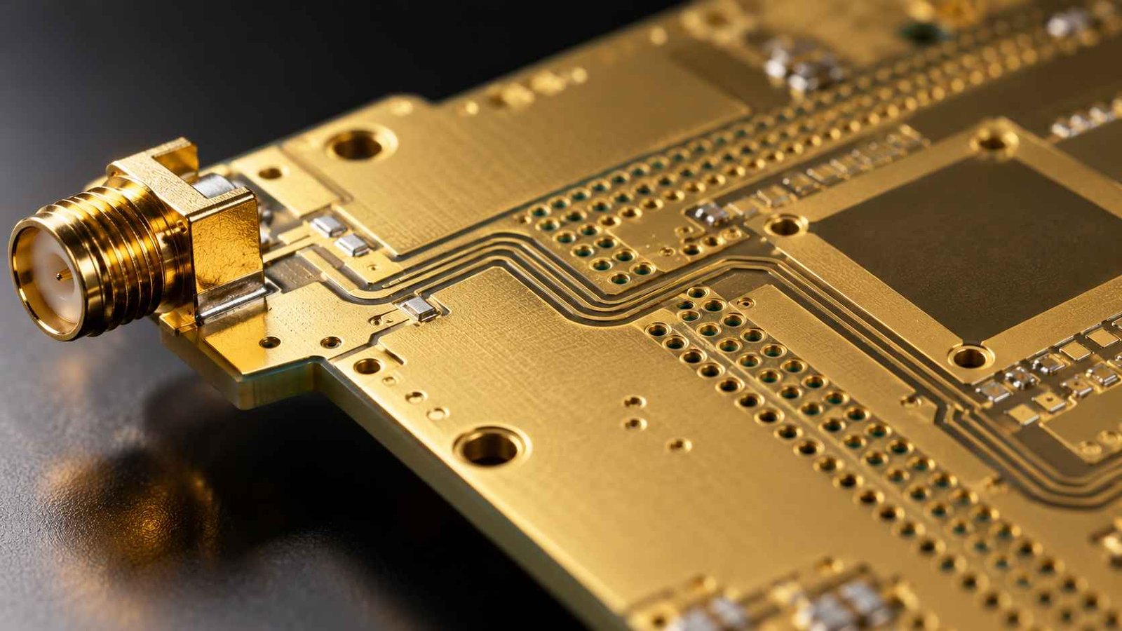
Common questions about high-frequency PCB design and fabrication.
Prioritize Dk below 3.5 and Df below 0.002 — for example Rogers RO4003C or PTFE-based laminates — to minimize signal delay and attenuation at GHz-level frequencies.
ENIG offers good planarity and solderability; immersion silver has lower loss but needs strict packaging against oxidation. Avoid HASL — its uneven surface increases high-frequency losses.
Unused via stubs act as resonant structures that cause signal reflections and interference. Back drilling removes the stub and is especially critical for signals above 5 GHz.
TDR impedance testing within ±10% tolerance, VNA S-parameter testing (S11 below -15 dB, S21 above -3 dB), and 3 IR reflow cycles at 260°C ± 5°C checking delamination below 5%.
Send us your design files and frequency band. Our engineering team will review your stack-up, impedance plan and surface finish, then quote your high-frequency PCB.
Request A DFM Review → Fast Reply on WhatsApp