The design rules that actually move the needle on GHz-level boards — low-loss materials, controlled impedance, stripline routing, back drilling and return-path discipline.
High-speed high-frequency PCB design has become essential across 5G communications, radar systems, aerospace electronics, automotive ADAS, satellite devices and AI data centers. As operating frequencies push into multi-GHz ranges, traditional design habits stop working — signal integrity, impedance control, electromagnetic compatibility and transmission loss all demand attention.
Unlike standard digital boards, RF and high-speed PCBs behave like controlled electromagnetic structures rather than simple electrical connections. Every trace, via, dielectric layer and reference plane directly affects signal quality.
This guide walks through the principles behind reliable high-speed high-frequency PCB design — and the board-level techniques that keep signals stable under extreme conditions.
Traditional FR-4 has relatively high dielectric loss (Df) at high frequencies — more electrical energy converts to heat, bringing signal attenuation, timing instability and poor insertion loss.
That is why manufacturers build RF boards on advanced low-loss laminates from Rogers, Taconic and Panasonic Megtron — materials offering low loss tangent (Df 0.0005–0.002), stable Dk (2.2–3.5), reduced insertion loss, better phase consistency and improved impedance stability.
Low-loss laminates are what keep signal fidelity alive in RF design, microwave circuits and high-speed digital interfaces above 10 Gbps.
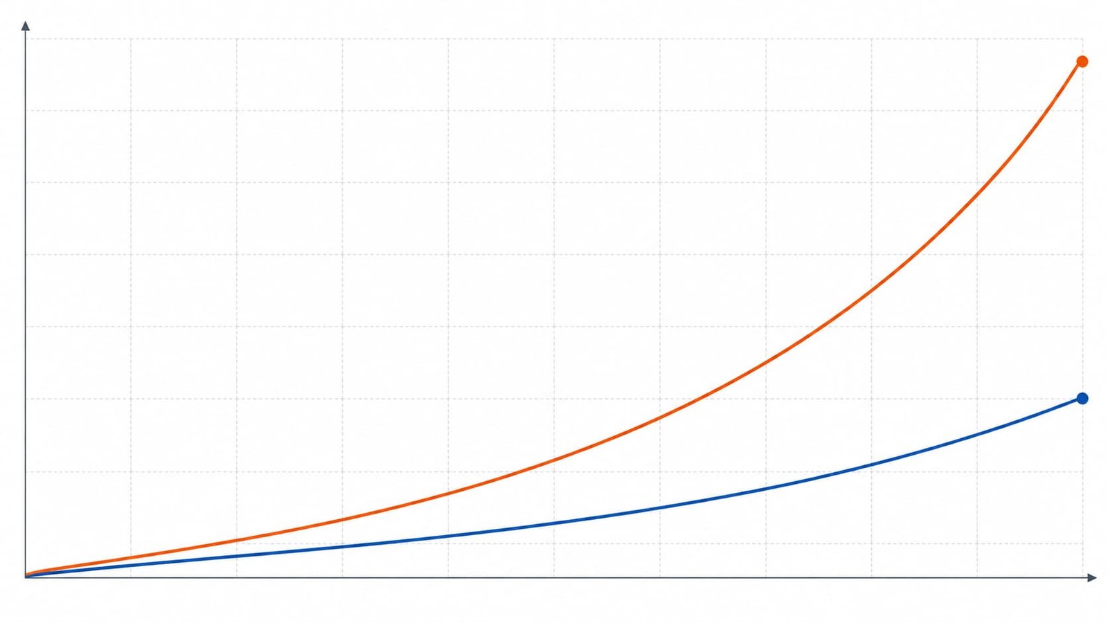
In high-speed layout, impedance is not just a target value — it has to hold within strict tolerance. Common controlled structures: 50Ω single-ended traces, 100Ω differential pairs, 85Ω USB routing and 90Ω LVDS interfaces. Modern RF fabrication typically holds impedance within ±5% or tighter.
Accurate matching minimizes reflection and maximizes power transfer between transmitter and receiver. Engineers get there by controlling trace width, copper thickness, dielectric thickness, PCB stack-up and material Dk values.
Without it: reflections, eye-diagram degradation, jitter and data errors.
Transmission-line structure choice is one of the most important decisions in high-speed design.
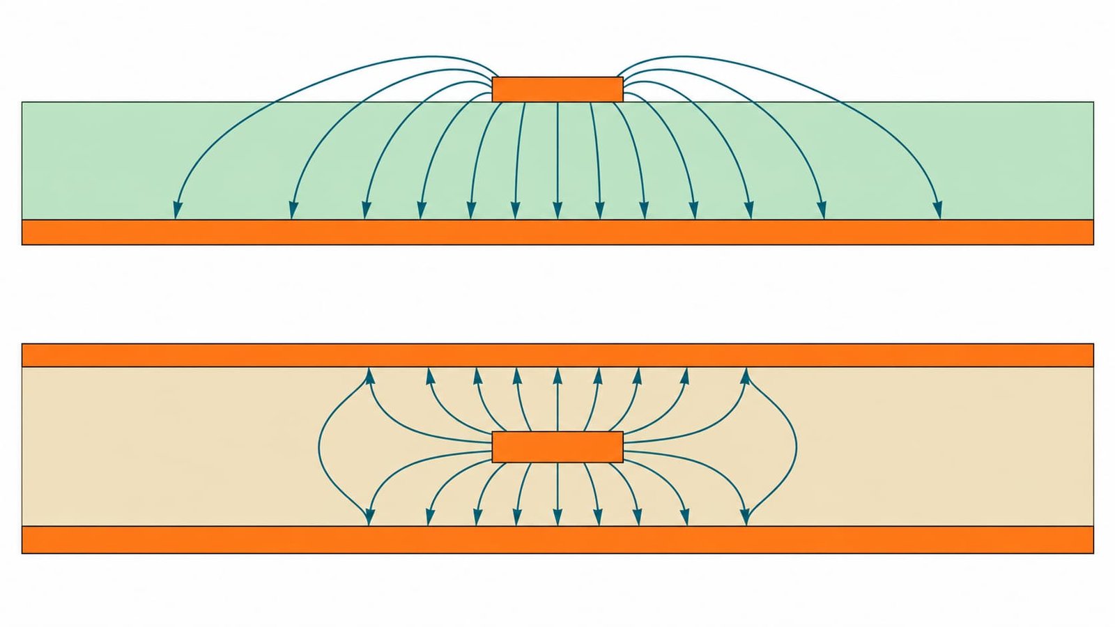
Microstrip traces sit on the outer PCB layer and reference a nearby ground plane. Advantages: lower propagation delay, easier tuning and debugging, lower manufacturing complexity. Disadvantages: higher EMI radiation and greater susceptibility to external interference.
Stripline traces are embedded between reference planes inside the board. Advantages: excellent shielding, extremely low radiation, better noise immunity. Disadvantages: higher insertion loss, more difficult fabrication and larger signal delay.
Most advanced multilayer designs use a combination of the two, depending on signal sensitivity and routing distance.
At GHz frequencies, even small routing discontinuities can create severe signal problems.
High-frequency traces should avoid 90-degree corners. Curved or arc routing reduces impedance discontinuities and minimizes harmonic radiation.
Differential pairs need extremely tight length matching between P and N traces — typically ≤0.5 mm or ≤5 mil. Proper matching synchronizes signal arrival times and reduces common-mode noise. Dense accordion-style serpentine routing should be avoided: it increases unwanted coupling and impedance variation.
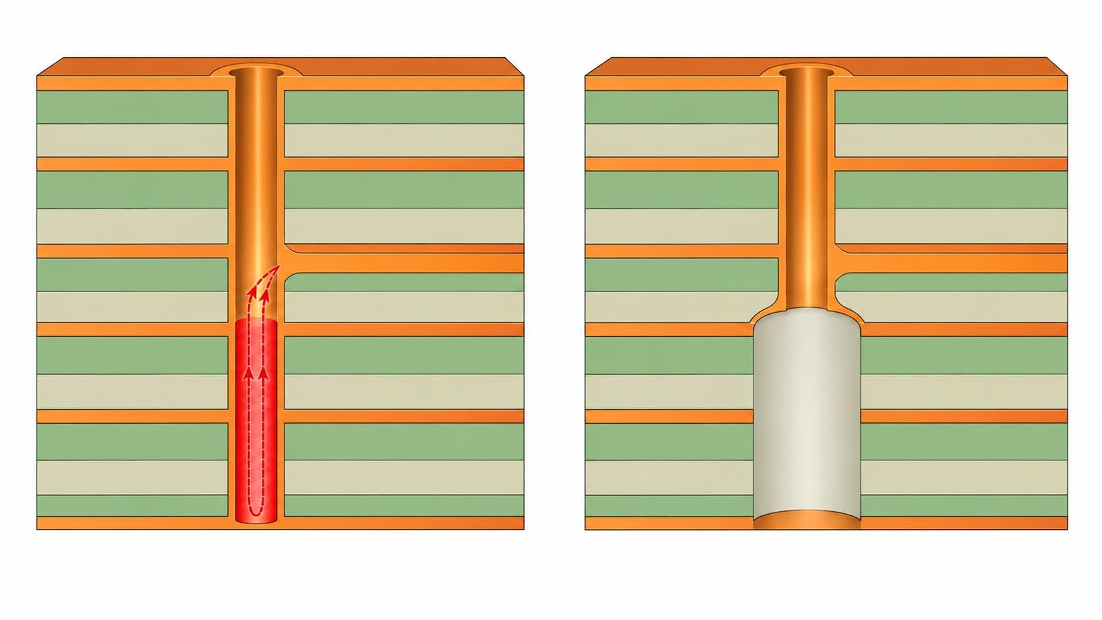
Vias introduce parasitic capacitance and inductance that become increasingly problematic at high frequencies.
Back drilling removes unused via stubs after layer transitions. Benefits: reduced signal resonance, lower reflection, improved insertion loss and wider usable bandwidth — essential for 10 Gbps, 25 Gbps and faster applications.
Modern high-density RF manufacturing uses 0.2 mm mechanical vias, laser microvias and HDI structures. Smaller vias reduce parasitic effects and improve signal transition quality.
Every high-speed signal needs a clean return current path. A continuous reference plane beneath signal traces minimizes loop inductance, reduces EMI radiation, lowers ground bounce noise and improves signal stability.
High-speed clock lines and RF signals should never cross split planes or gaps in the reference layer — the return-current detour creates electromagnetic interference problems. Ground via stitching is also widely used to build low-inductance return paths and improve shielding.
In many RF applications, solder mask is removed from critical RF traces — conventional mask materials have unstable dielectric properties and higher loss at microwave frequencies.
Common high-frequency surface finishes include ENIG, immersion silver and OSP. Because of skin effect, high-frequency current flows only along the conductor surface — smooth finishes significantly cut conductor loss.
As signal density increases, crosstalk and EMI become major challenges.
Adjacent traces should maintain spacing of at least three times the trace width to reduce electromagnetic coupling.
Additional suppression methods include ground copper along PCB edges, via fencing, RF shielding covers and microwave absorbing materials — together they contain radiation and improve overall EMC performance.
High-speed high-frequency PCB design is fundamentally about controlling electromagnetic wave behavior inside the board. Every decision — low-loss materials, controlled impedance, back drilling, return-path discipline — lands directly on signal quality and system reliability.
As data rates keep climbing and communication systems push deeper into microwave frequencies, these techniques stop being optional. If you are planning a GHz-level build, start with our high-frequency PCB fundamentals, then have our team review the design before it goes to production.
Common questions about high-speed high-frequency PCB design.
A board operating above roughly 1 GHz, handling RF, microwave or high-speed digital signals where loss and interference must be actively managed rather than tolerated.
Its dielectric loss climbs and its Dk drifts at high frequency, so signals attenuate and timing becomes inconsistent — acceptable below 1 GHz, risky above it.
It keeps the transmitter, the trace and the receiver matched. Without it you get reflections, degraded eye diagrams and data errors that no amount of firmware tuning will fix.
It removes the unused via stub left after layer transition — that stub acts like a small resonant antenna, wrecking insertion loss at high data rates.
ENIG and immersion silver are the usual choices, because they leave a smooth conductive surface — which matters once skin effect confines current to the conductor surface.
Send us your stack-up, impedance targets and data rates. Our engineering team will review the design for manufacturability and quote your high-speed board.
Get A Design Review → Fast Reply on WhatsApp