High-Frequency PCB Insights & Resources

Technical guides, material comparisons and process insights on high-frequency, RF and microwave PCB manufacturing.

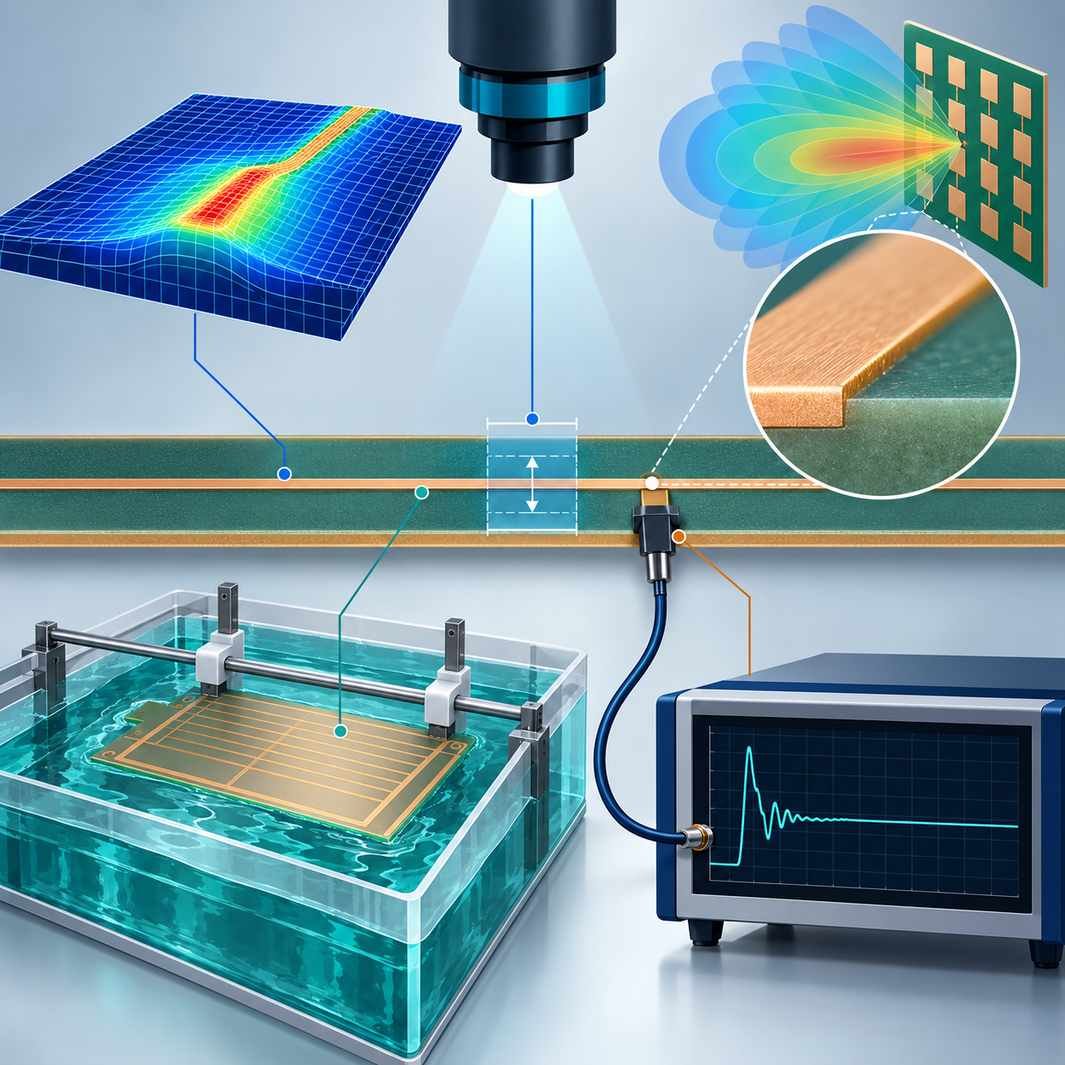
Extremely narrow microstrip trace under a caliper bracket with simulation, imaging, etching and TDR verification links and a 5G antenna inset

High-Frequency PCB Microstrip Line Design: How to Ensure Impedance Consistency with 0.05mm Line Width?

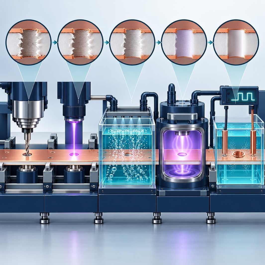
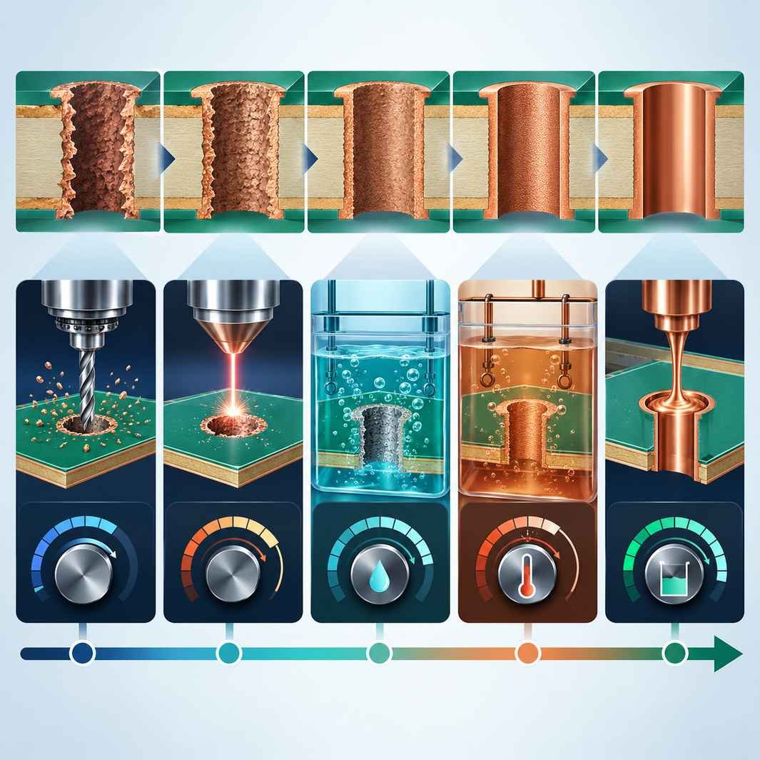
Five-station PTFE hole wall quality chain from drilling and laser drilling through chemical etching, plasma treatment and pulse plating

Rough Hole Walls in High-Frequency PCBs? 5 Solutions to Boost PTFE Metallization Reliability

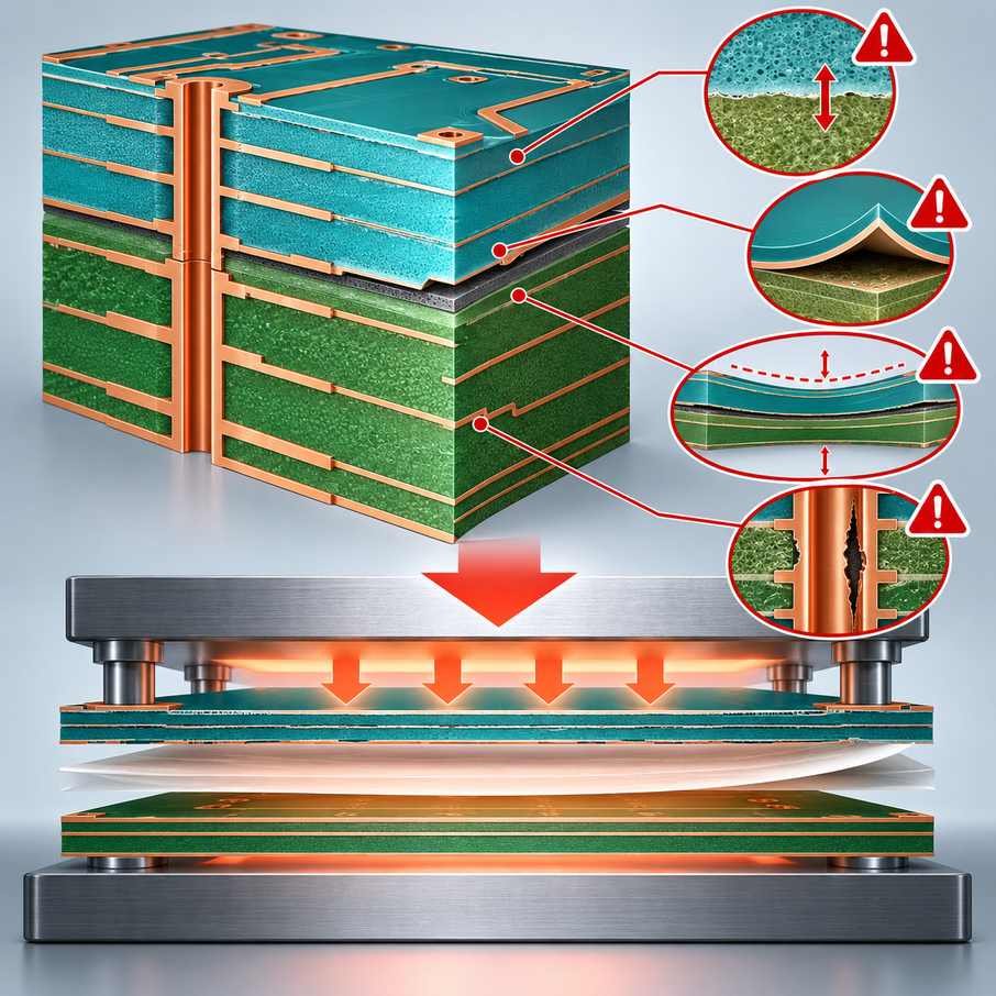
RO5880 and FR-4 hybrid stack cross-section with four interface warning markers for dielectric mismatch, weak bonding, warpage and plating voids

Hybrid PCB Stack-up Analysis: Key Process Considerations for Rogers RT5880 and FR4 Integration

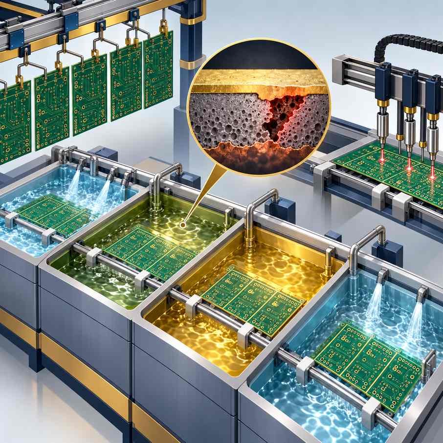
ENIG plating line with micro-etch, nickel and gold baths, a magnified porous corrosion pocket and plating uniformity probes

ENIG Plating for High-Frequency PCBs: Process Optimization to Prevent Black Pad and Plating Defects

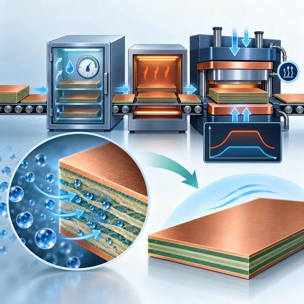
Four-stage moisture control chain for PTFE boards from sealed storage and baking through lamination profile to low-moisture laminate alternatives

Delamination and Blistering in High-Frequency PCBs: Solving Moisture Absorption & Lamination Issues

Five PTFE hole wall improvement methods as parameter cards with drilling, laser, chemistry, electroless copper and via filling dials

5 Effective Methods to Improve Hole Wall Quality in PTFE High-Frequency PCBs

Three root causes of rough PTFE hole walls mapped to drilling, chemistry and laser countermeasure cards with a decision fork below

5 Proven Methods to Improve Hole Wall Quality in PTFE High-Frequency PCBs

Complete ENIG line of seven stations for RF PCBs with three uneven plating pattern coupons and a final RF test bench

Comprehensive Guide to ENIG Process for High-Frequency PCBs: Preventing Black Pad & Plating Defects

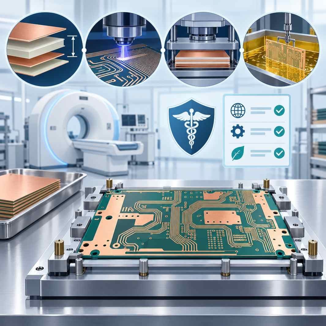
Four signal integrity technologies for medical-grade high-frequency PCB manufacturing, with a medical scanner, certification seal and supplier checklist

Medical-Grade High-Frequency PCB Manufacturing: Ensuring Signal Integrity

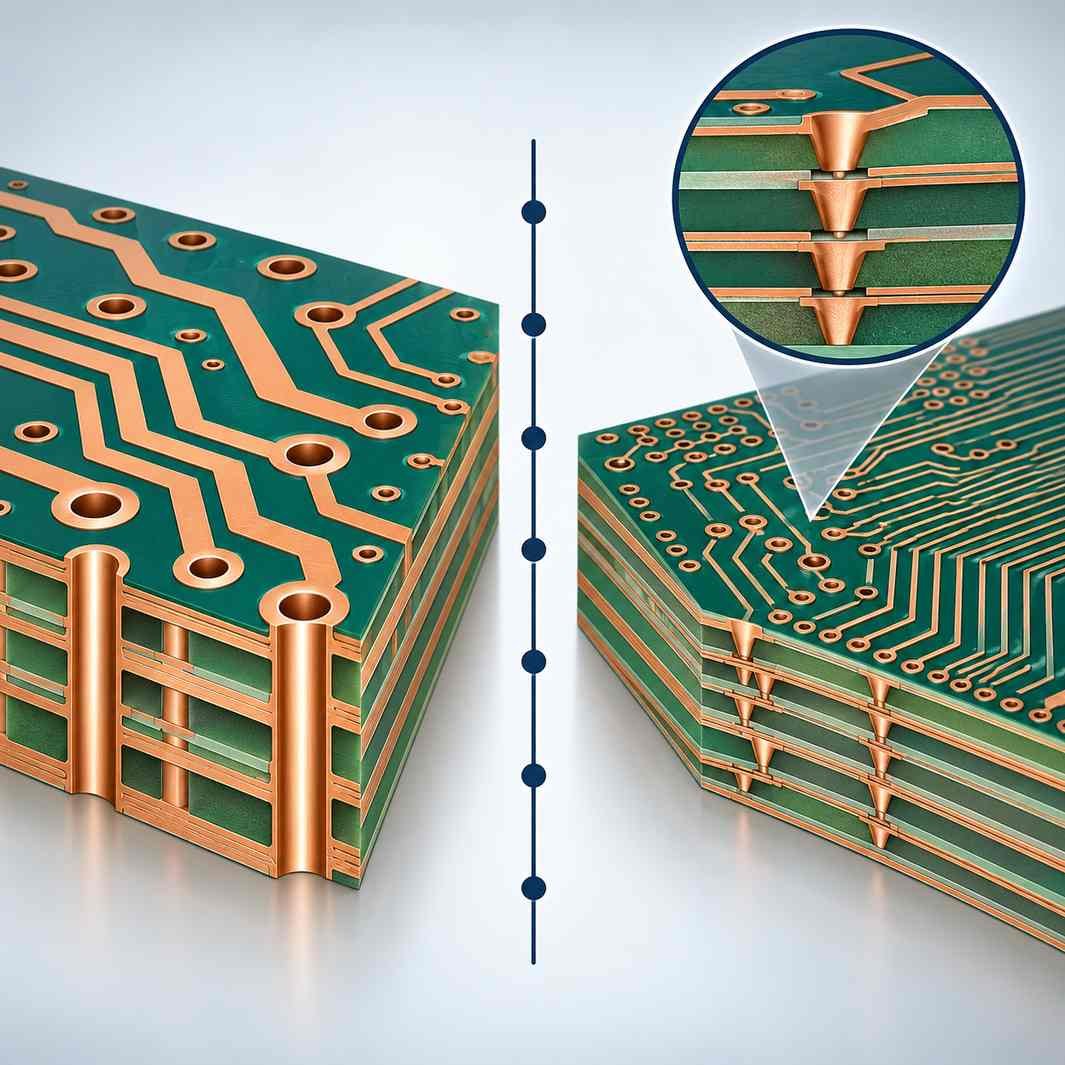
Traditional multilayer board beside a denser HDI board with stacked microvias, separated by six comparison tick marks

HDI PCB vs Traditional PCB: Comprehensive Technical Comparison & Selection Guide

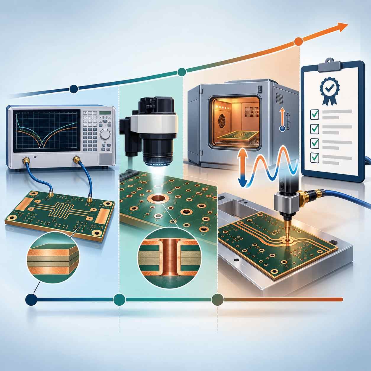
Three-phase reliability workflow timeline from design verification and in-process control to final environmental and RF validation

Comprehensive Reliability Testing for High-Frequency PCBs: Key Standards from Impedance Control to Thermal Aging

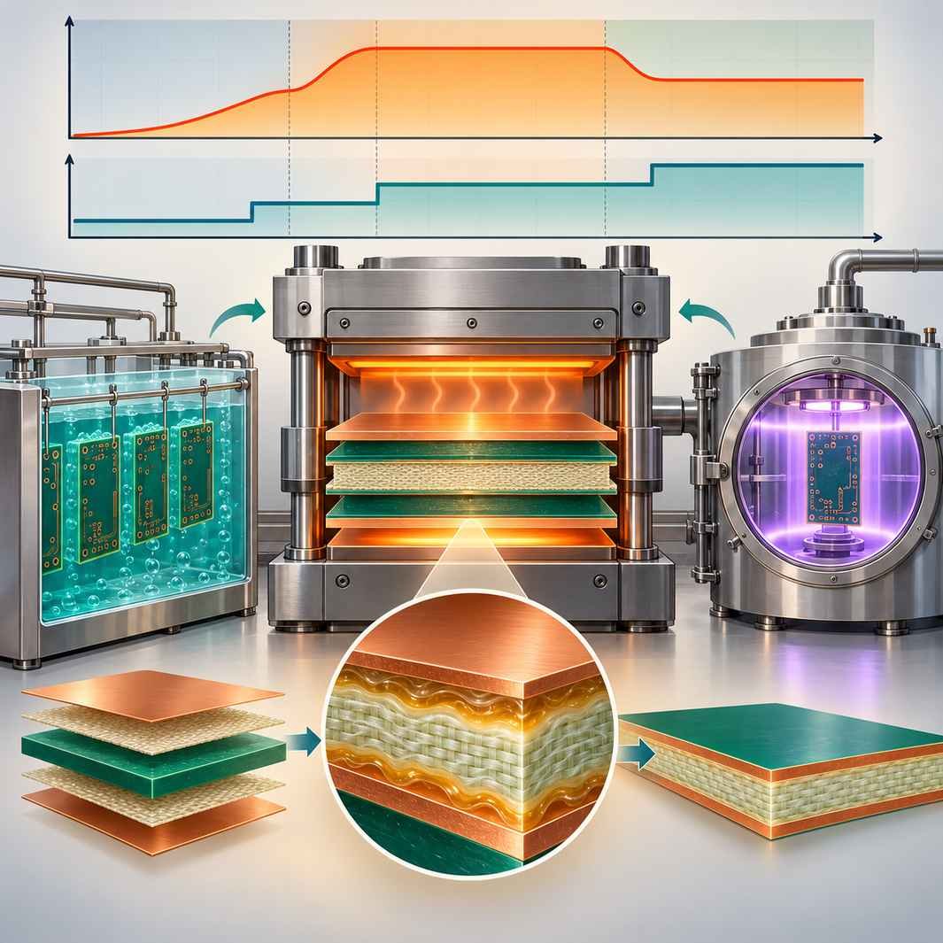
F4B and FR4 hybrid stack in a lamination press with temperature profile, three-step pressure staircase and surface treatment stations

F4B Hybrid Lamination Guide: Optimizing Temperature & Pressure for FR4 Combinations

PCB Assembly

PCBA Services

Quality

Application

Resources

Printed Circuit Board

RF PCB

Quality

PCB Surface Finish

Printed Circuit Board

Drills & Throughplating

Profiles

PCB Stackup

Resources