
Steps and Considerations for Impedance Control in High-Frequency PCB Manufacturing

Steps and Considerations for Impedance Control in High-Frequency PCB Manufacturing From design calculation and simulation to TDR verification — the seven steps and five disciplines that keep impedance inside tolerance on high-frequency PCBs. Table of Contents Impedance control is crucial for signal integrity and circuit performance in high-frequency PCBs, especially in applications involving RF, microwave, […]
Finished Product Testing and Environmental Simulation Equipment in the Production Process of High-Frequency PCBs
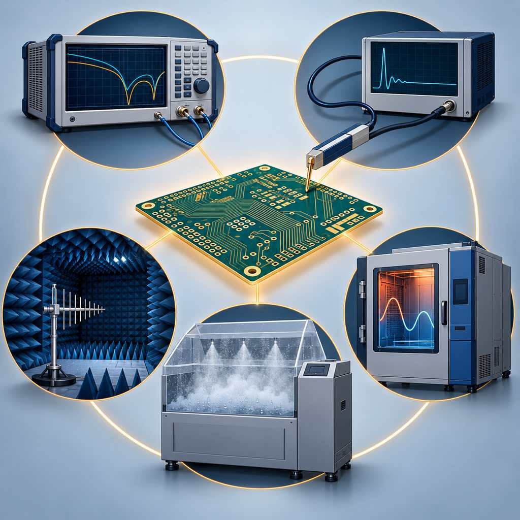
Finished Product Testing and Environmental Simulation Equipment in the High-Frequency PCB Factory Network analyzers, TDR, thermal cycling, salt fog and EMI chambers — the test and environmental simulation equipment that guarantees high-frequency PCB reliability. Table of Contents With the rapid development of fields such as high-frequency communication, 5G, satellite navigation, and radar technology, the application […]
Post-Processing Steps and Considerations in High-Frequency PCB Production
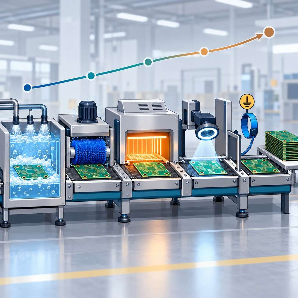
Post-Processing Steps and Considerations in High-Frequency PCB Production Cleaning, deburring, drying, inspection and ESD control — the post-processing steps, common failure modes and emerging trends behind reliable high-frequency PCBs. Table of Contents Post-processing is the final gate of high-frequency PCB production: the cleaning, finishing and inspection steps that happen after plating, etching and soldering. Done […]
High-Frequency PCB Production: Steps and Considerations for Microstrip and Stripline Design
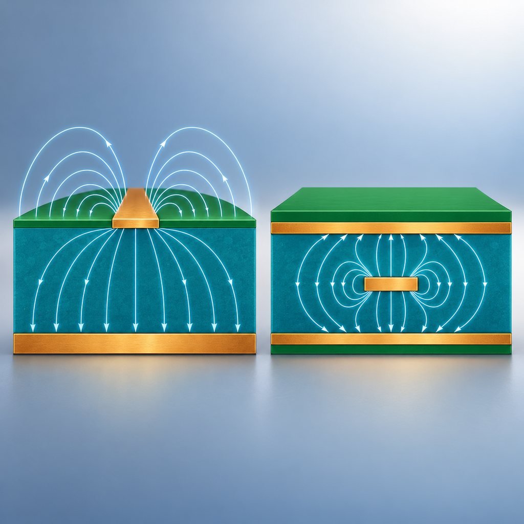
High-Frequency PCB Production: Steps and Considerations for Microstrip and Stripline Design From impedance targets and substrate selection to simulation, tolerances, and the four most common failure modes — a practical walkthrough of microstrip and stripline design in high-frequency PCB production. Table of Contents Basic Concepts of Microstrip and Stripline Microstrip: A widely used transmission line […]
Steps and Considerations for Surface Treatment in High-Frequency PCB Production
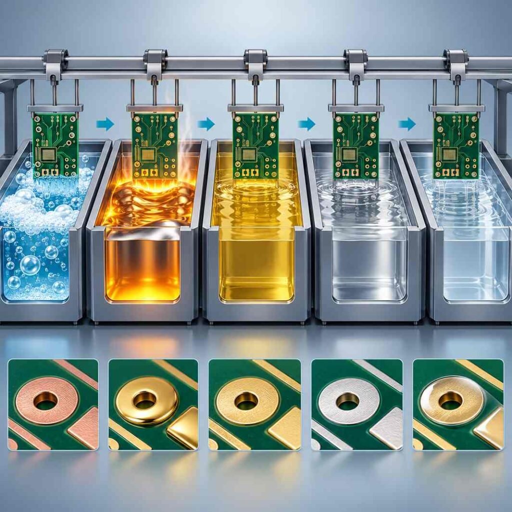
Steps and Considerations for Surface Treatment in High-Frequency PCB Production The five process steps from cleaning to testing, key control points, and an honest comparison of HASL, ENIG, tin, silver and coating treatments — plus fixes for the four most common plating defects. Table of Contents Main Steps in Surface Treatment Surface treatment directly affects […]
Laser Engraving and Marking Equipment in High-Frequency PCB Manufacturing
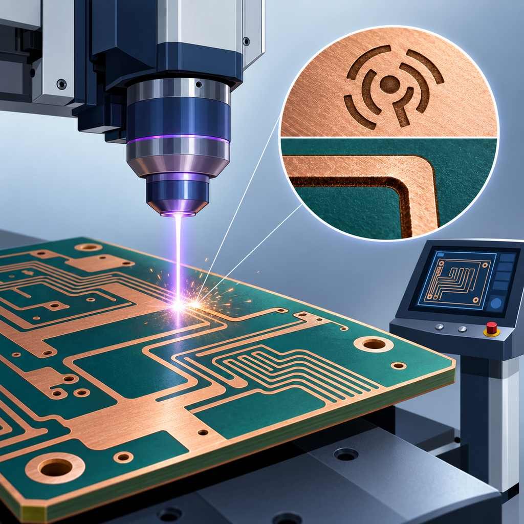
Laser Engraving and Marking Equipment in High-Frequency PCB Manufacturing How laser engraving and marking works, where it fits in high-frequency PCB production — pad engraving, trace cutting, traceability marking — and the five advantages that make it indispensable. Table of Contents Overview of Laser Engraving and Marking Equipment Laser engraving and marking equipment directs a […]
Optical Microscopes and Electron Microscopes in High-Frequency PCB Manufacturing
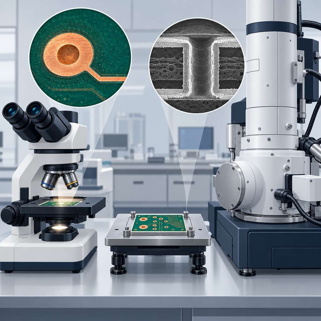
Optical Microscopes and Electron Microscopes in High-Frequency PCB Manufacturing Working principles, five application areas from BGA inspection to micro-via analysis, and when each microscope technology earns its place on the production floor. Table of Contents Overview: Optical Microscopes vs Electron Microscopes Optical microscopes magnify objects with an optical lens system using visible light. They are […]
Laser Etching Machine in High-Frequency PCB Production Process
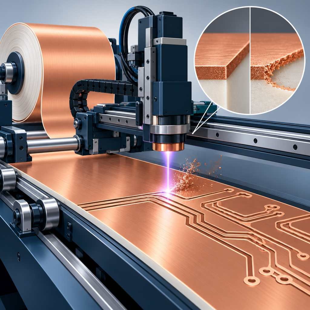
Laser Etching Machine in High-Frequency PCB Production Process How laser etching machines form circuit patterns on PTFE, ceramic and polyimide laminates — working principles, five applications, and why they outperform chemical etching for high-frequency work. Table of Contents Overview of Laser Etching Machines In high-frequency PCB production, etching is the step that forms the circuit […]
High-Precision Lithography Machines (Exposure Machines) in High-Frequency PCB Production
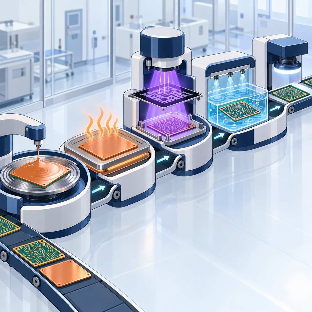
High-Precision Lithography Machines (Exposure Machines) in High-Frequency PCB Production The five-stage lithography workflow from photoresist coating to post-processing, four application areas, and why micron-level pattern transfer defines quality in high-frequency PCB production. Table of Contents Overview of High-Precision Lithography Machines A high-precision lithography machine (exposure machine) transfers circuit design patterns onto the PCB surface using […]
Processing Considerations for High-Frequency PCBs
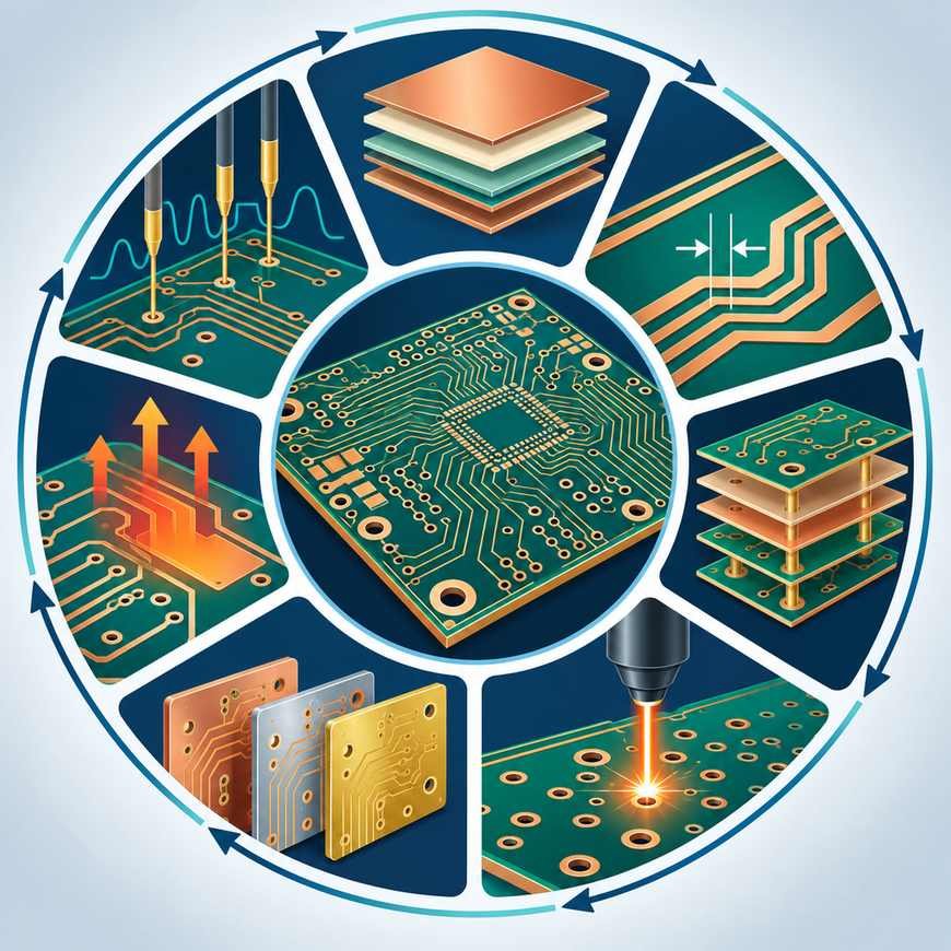
Processing Considerations for High-Frequency PCBs Seven control points from material selection and line-width precision to lamination, drilling, surface treatment, thermal management and signal integrity testing. Table of Contents Material Selection The substrate material significantly influences high-frequency PCB performance. Common choices include PTFE (polytetrafluoroethylene), ceramic-filled compounds, and composite materials — all offering low dielectric constants and […]
Considerations in the Production Process of Microwave PCBs
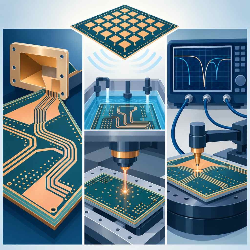
Considerations in the Production Process of Microwave PCBs Design rules for materials, layout and impedance matching, manufacturing control points for etching and drilling, plus the electrical and environmental tests that validate every microwave PCB. Table of Contents Overview of Microwave PCBs Microwave PCBs are designed for the transmission and processing of microwave-frequency signals (typically 1 […]
Exploring the Superior Performance and Production Artistry of Rogers RO3003C Laminate
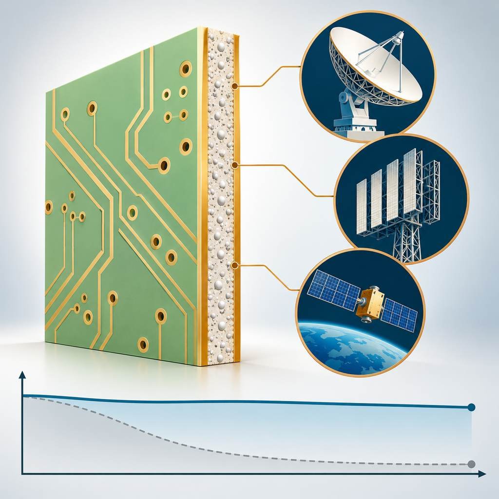
Exploring the Superior Performance and Production Artistry of Rogers RO3003C Laminate Why ceramic-filled PTFE wins at millimeter-wave: Dk stability of 3.00 ± 0.04, 20× lower loss than FR-4, drilling and lamination precautions, and real deployments from 77 GHz radar to 100 Gb/s links. Table of Contents Background: Material Challenges in the High-Frequency Era As communication […]