High-Frequency PCB Insights & Resources

Technical guides, material comparisons and process insights on high-frequency, RF and microwave PCB manufacturing.

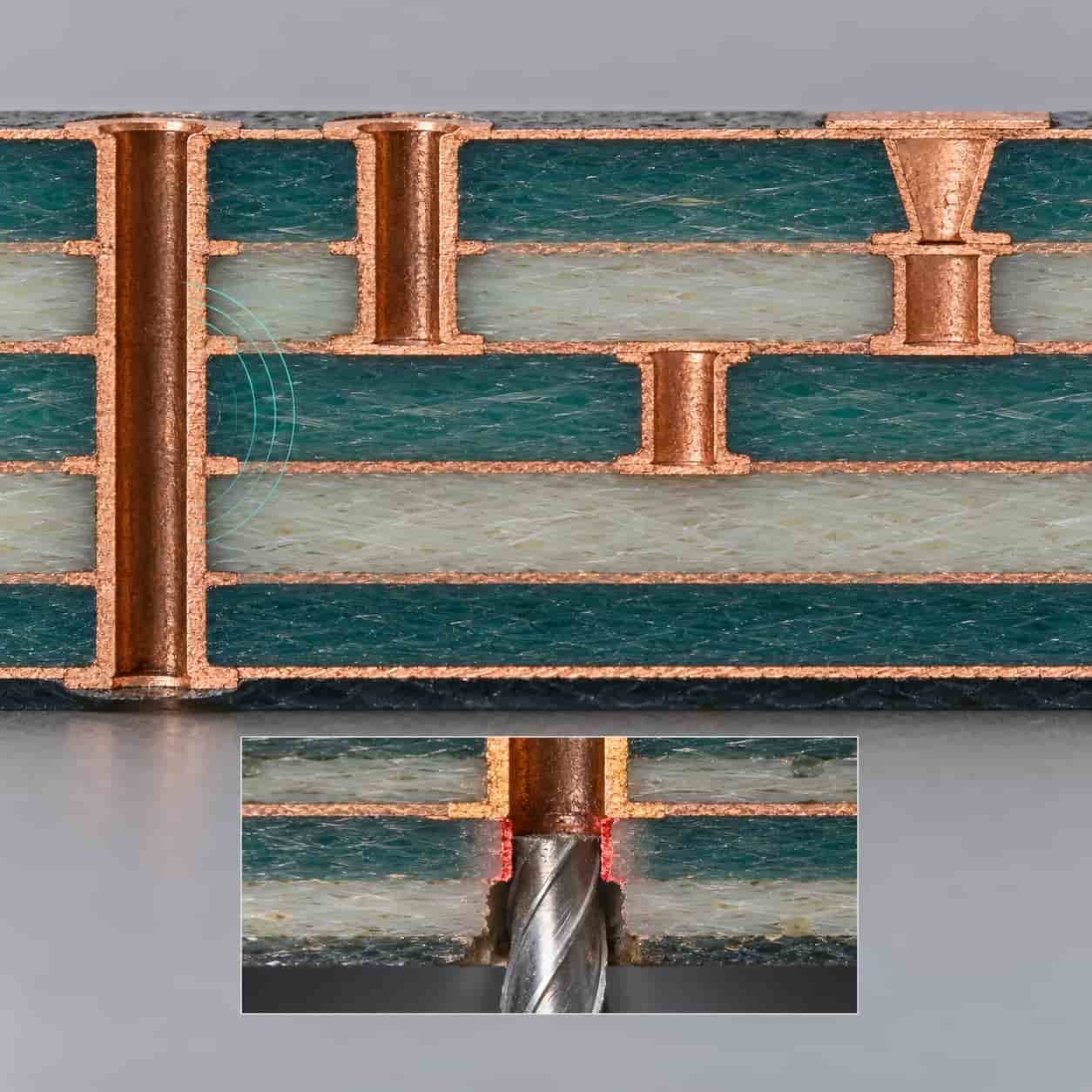
Four via structures in a multilayer cross-section with a back-drilling tool removing a stub and parasitic arcs beside a via

PCB Via Guidelines for Multi-layer Circuit Board Manufacturing

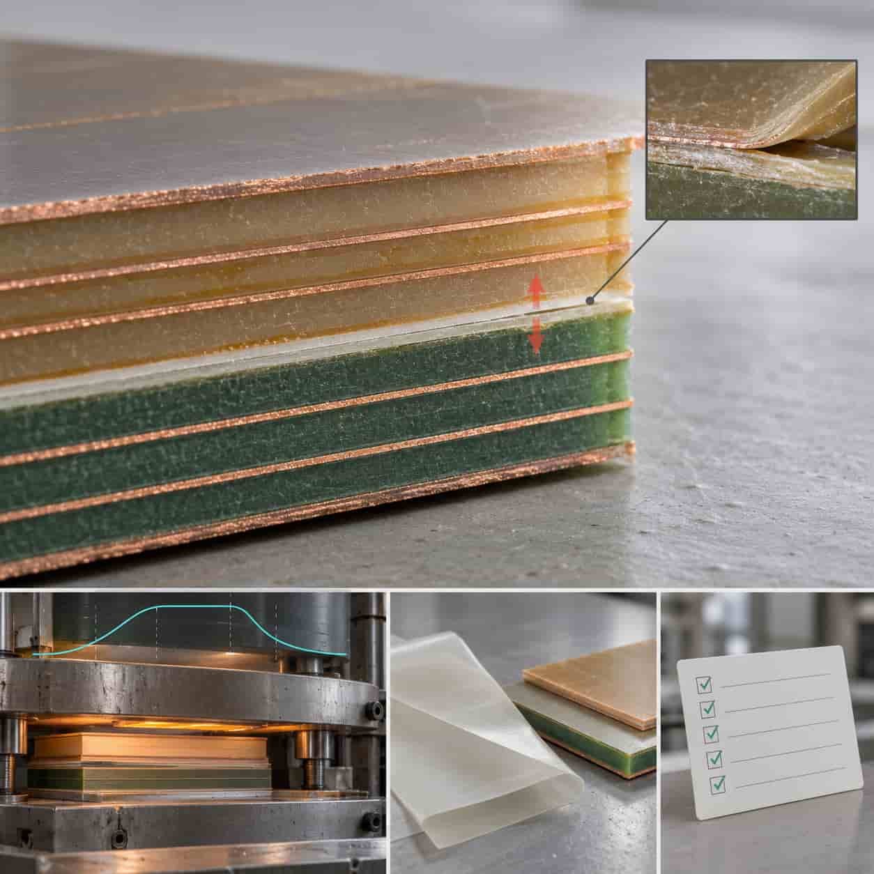
Hybrid PCB stack with high-frequency and FR-4 layers, CTE mismatch and delamination warnings and a lamination fix with specification checklist

Why Use a Hybrid PCB? Hybrid PCB Design and Manufacturing Process

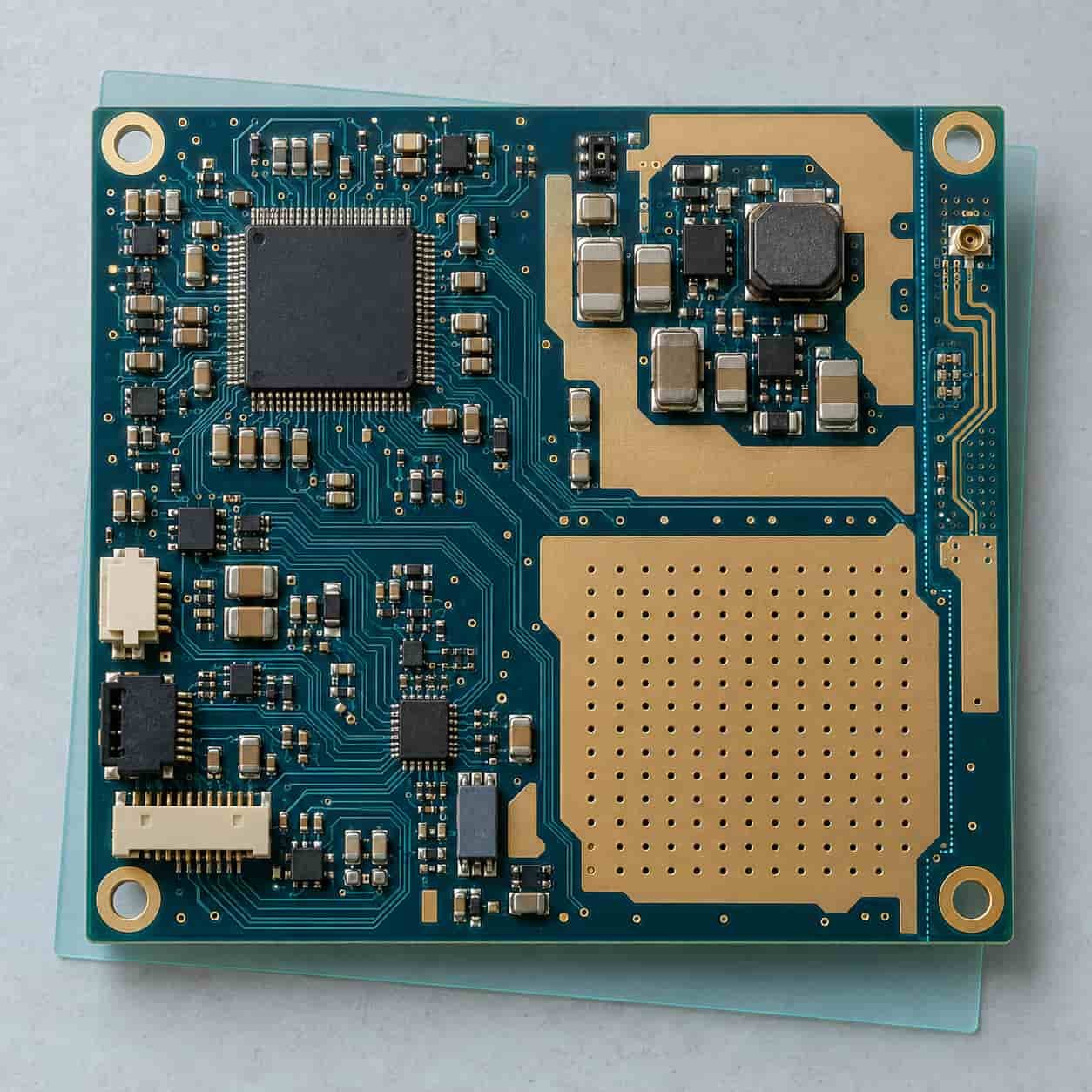
PCB layout with placement zoning for processor decoupling, power rails, connectors and thermal vias above a reference plane sheet

Standard PCB Layout Guidelines

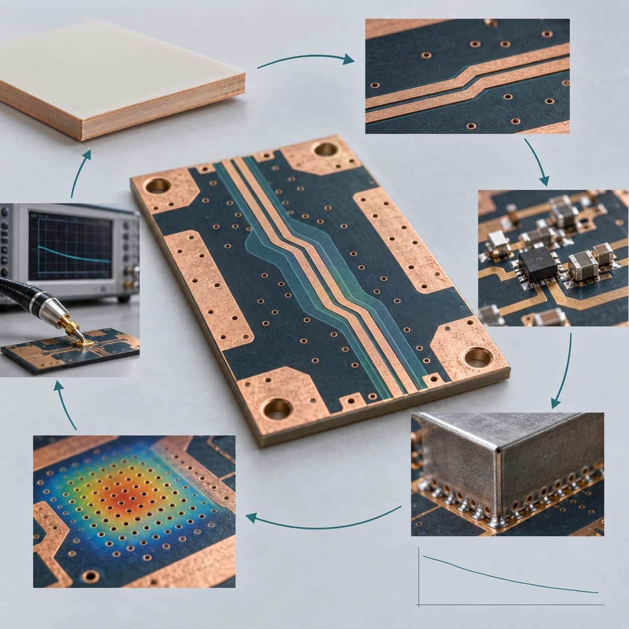
Six-step RF PCB design ring from material and transmission lines through placement, grounding, thermal and validation

RF PCB Design Guidelines and Considerations

Five supplier evaluation dimensions around a high-frequency board with an engagement timeline from concept to volume and an RFQ card

How to Find an RF PCB Manufacturer and When to Engage Them

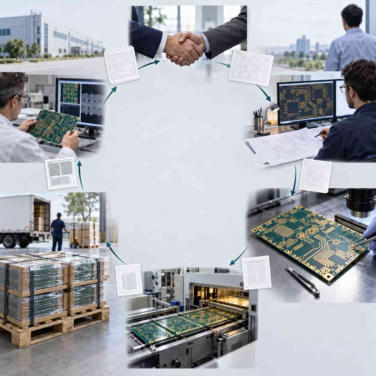
Six-stage collaboration lifecycle ring between a customer and a PCB factory from selection and design through prototype, volume and feedback

High-Frequency PCB Manufacturer Collaboration Process and Stages

In-process control lattice of five inspection nodes around a high-frequency board covering material, impedance, etch, hole wall and finish

Quality Assurance in the manufacturing of high-frequency PCBs (HF PCBs)

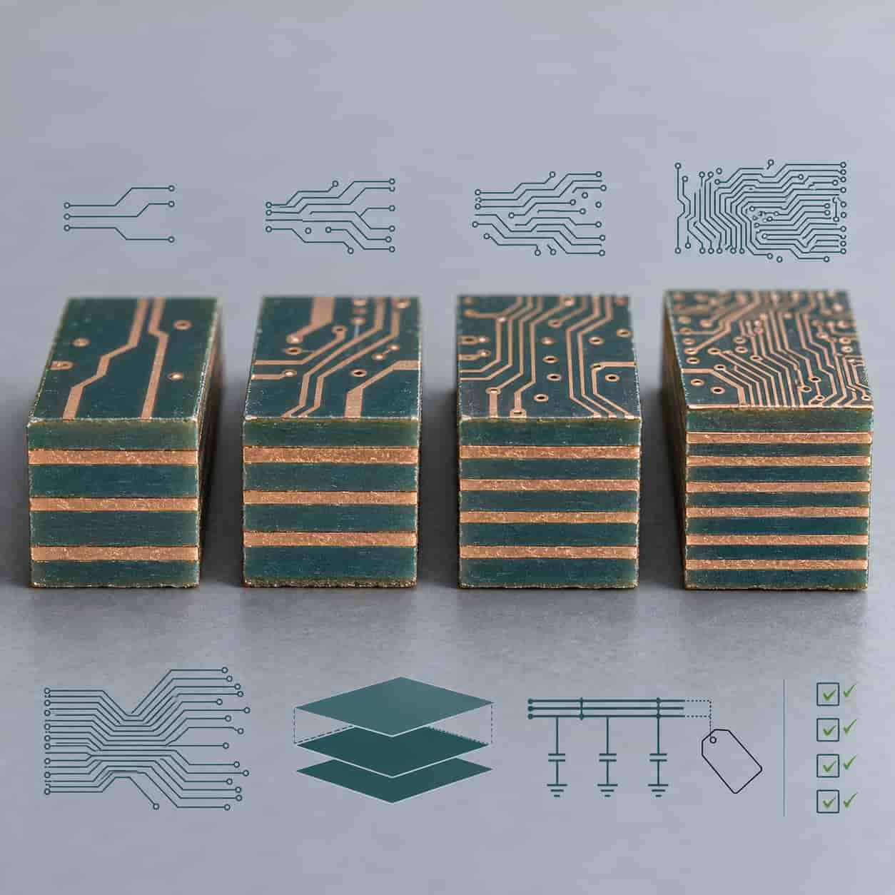
Four to eight layer PCB stack-ups in a row with routing density indicators and reference plane, power and cost drivers below

Multi-layer PCB Layer Count Design Principles

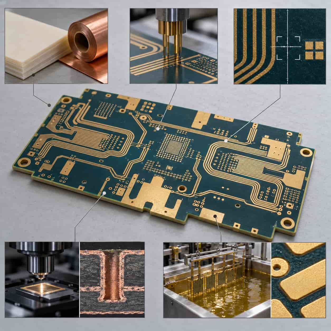
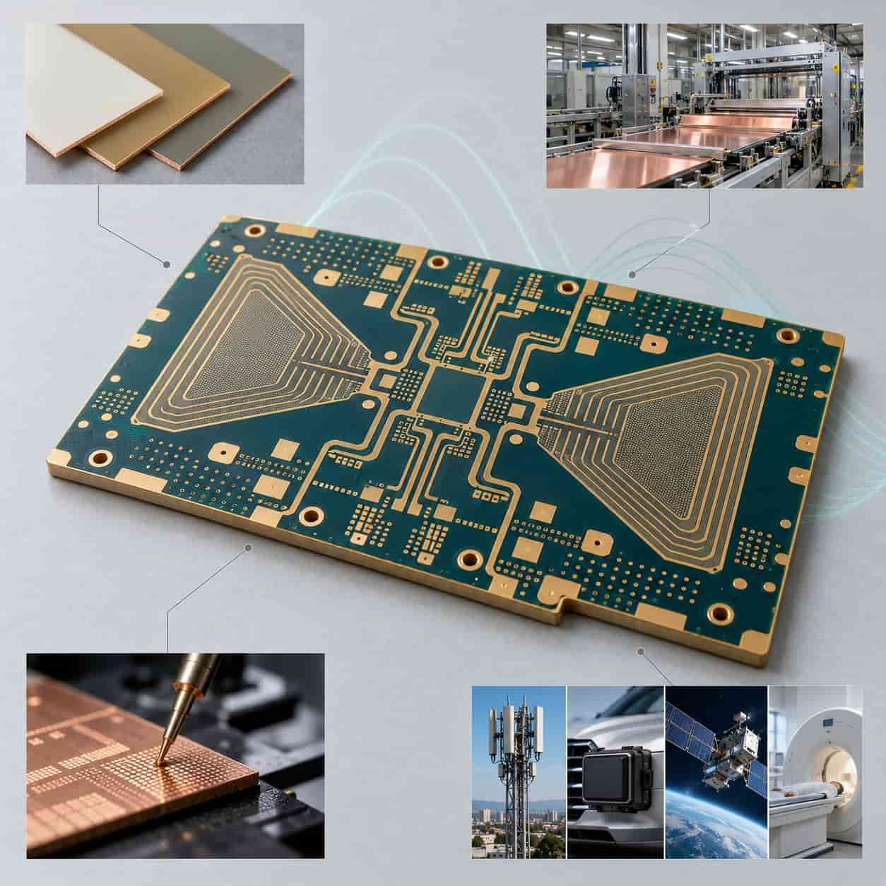
High-frequency PCB with callouts for material families, manufacturing, testing and applications across base station, radar, satellite and medical

What is High-Frequency PCB ?

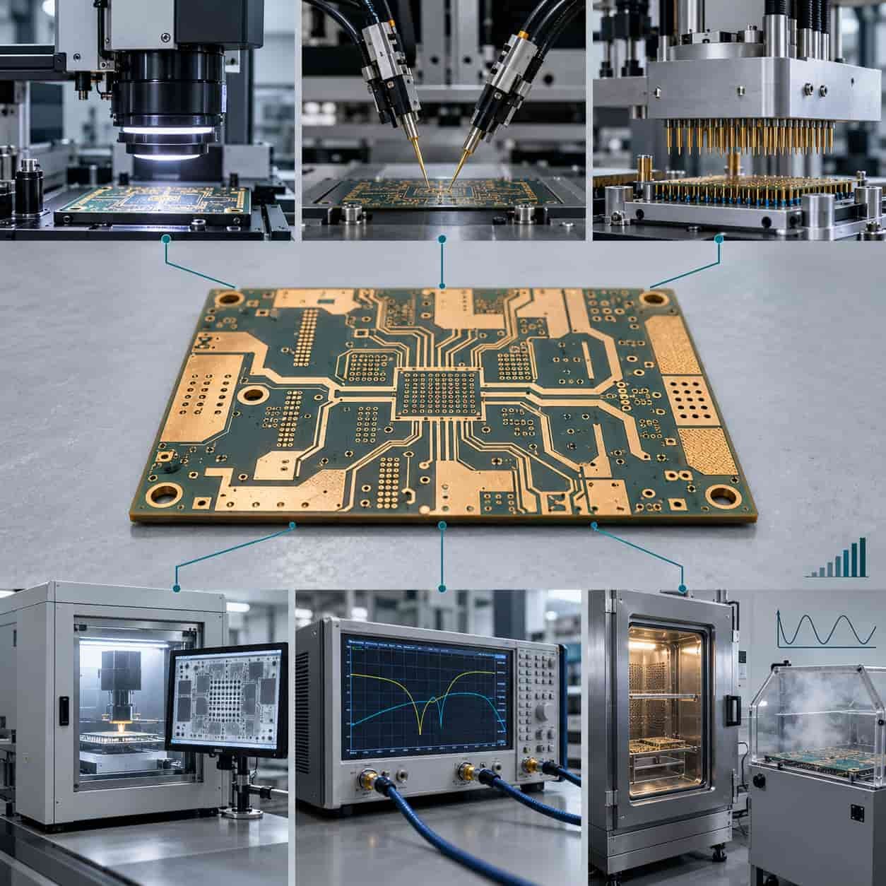
Six high-frequency PCB test families from AOI and flying probe through ICT, X-ray, functional RF and environmental testing

Testing and Inspection Processes for High-Frequency PCB Manufacturing

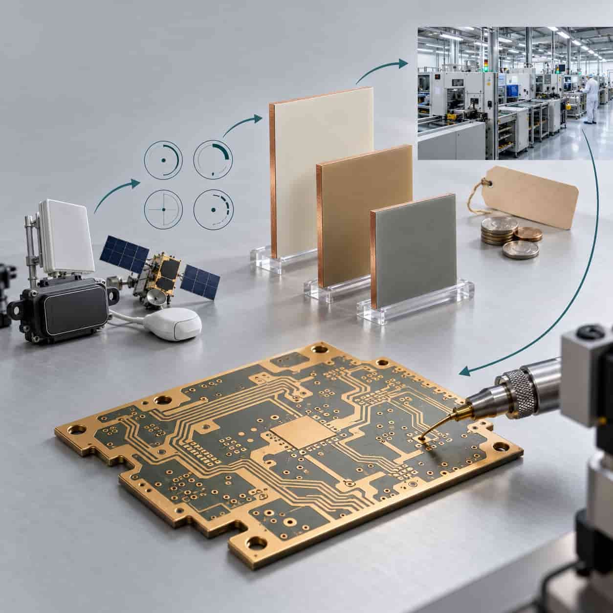
Four-stage PCB selection sequence from application demands through parameters and material families to manufacturability and validation

Selecting PCBs for RF and Microwave Applications

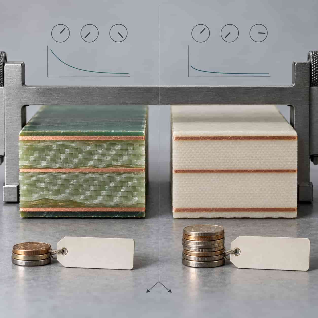
FR-4 board cross-section with woven glass beside an engineered high-frequency laminate, compared on parameter dials, loss curves and cost tags

FR4 substrates vs high-frequency materials

PCB Assembly

PCBA Services

Quality

Application

Resources

Printed Circuit Board

RF PCB

Quality

PCB Surface Finish

Printed Circuit Board

Drills & Throughplating

Profiles

PCB Stackup

Resources