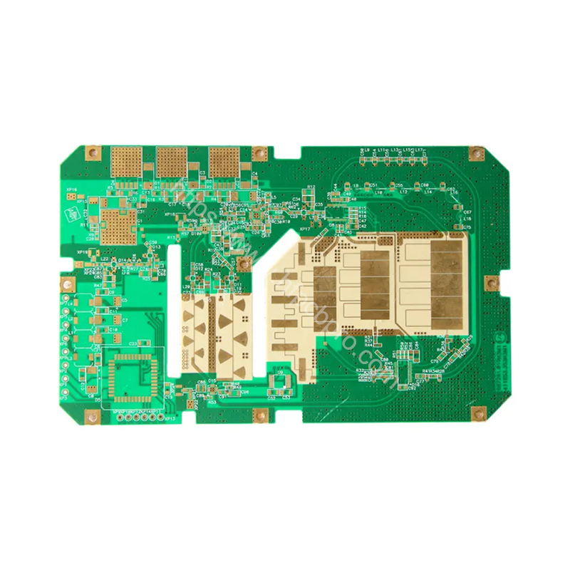
| Number of layers | 4L |
|---|---|
| Material | Rogers Ro6002 |
| Board Thickness | 1.6mm(65mil) |
| Quanlity Standard | GJB362B |
| Dielectric Constant (Dk) | 2.94 @10GHz |
| Dissipation Factor (Df) | 0.0012 @10GHz |
| Applications | |
| Surface Finish | ENIG 3u |
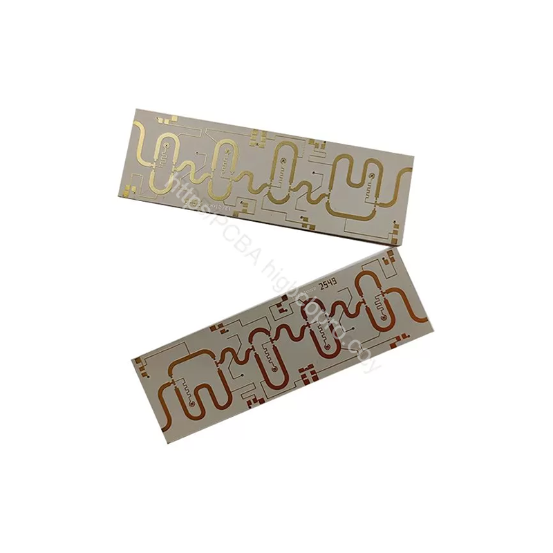
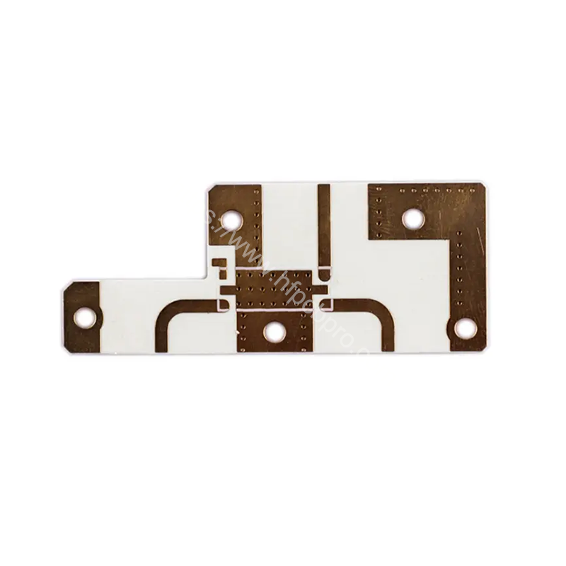
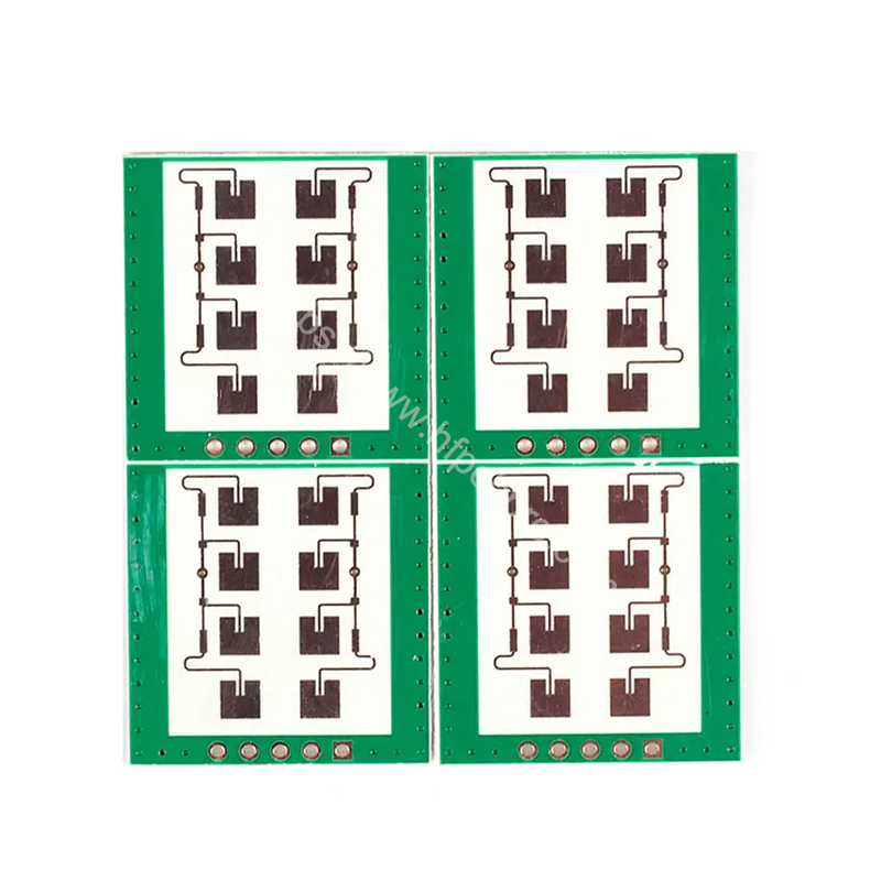
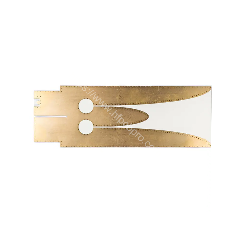
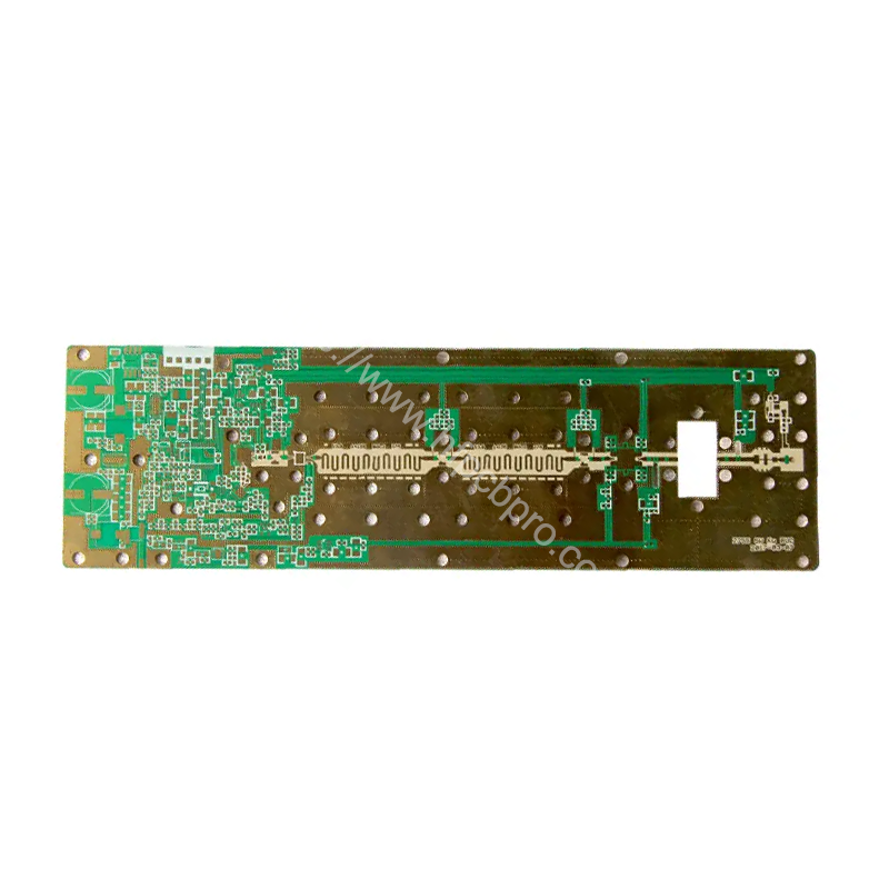
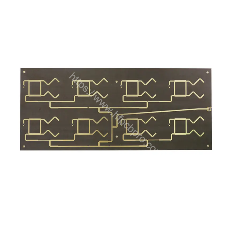
This four-layer RF microwave circuit board is listed with Rogers RO6002 laminate. The construction may suit microwave applications where controlled dielectric properties and a qualified multilayer stackup are required. Detailed performance depends on copper type, layer arrangement, trace geometry and fabrication process.
Data verification: These values come from the product’s current WordPress attributes. Verify the exact Rogers material data and measurement conditions against its datasheet before using them for impedance calculations or procurement.
Confirm the layer stackup, bonding materials, copper cladding, via structure and impedance targets before production. A manufacturability review should cover drilling, hole-wall treatment and lamination compatibility for the specified construction.
Review our Rogers PCB materials guide or send your files for an RF PCB quotation.
We offer a variety of high-frequency materials, including Rogers (e.g., RO4350B, RO5880), Taconic, and PTFE, depending on customer requirements.
Absolutely, we can provide detailed datasheets for review.
Our high-frequency PCBs can support frequencies up to 110 GHz, depending on the design and materials used.
We ensure precise impedance control through accurate stackup design, detailed impedance simulations, and advanced manufacturing processes.
Yes, we can combine materials like FR4 and high-frequency laminates for hybrid PCBs.
Restrictions mainly involve minimum trace width/spacing and material selection, depending on your design requirements.
We enhance thermal performance by using high thermal conductivity materials (e.g., metal-based PCBs) and optimizing copper thickness.
Thermal conductivity ranges from 0.2 W/m·K to 1.0 W/m·K, depending on the material.
ENIG/Gold Plating/Immersion Silver/Silver Plating/HASL/Gold finger/OSP/Nickel-palladium Gold/Resin plugging/Countersinking/ENIG+Hard Gold Plating/ImNi+ImTin/ENIG+OSP
ENIG is recommended due to its flat surface and excellent conductivity for high-frequency use.
We can produce high-frequency PCBs with layers ranging from 2 to 72.
Yes, we specialize in multilayer high-frequency PCBs and support hybrid stackup processes.
The thickness tolerance is ±0.05 mm, and the trace width tolerance is ±10%.
We perform impedance testing, RF performance testing, vacuum thermal testing, and more.
We achieve this by using high-quality materials, optimized manufacturing processes, and strict control of board thickness and other parameters.
Answer: Prototypes typically take 2–7 business days, while mass production takes 6–15 business days, depending on order volume and complexity.
High-frequency materials (e.g., Rogers) are more expensive, and higher layer counts increase complexity and cost.
We ensure reliability by using high-quality materials, rigorous testing, and optimized manufacturing processes.
Yes, our PCBs can endure temperatures up to 260°C and are suitable for harsh environments.
We use anti-static bags, vacuum packaging, and shockproof padding in the outer cartons for protection.
We provide air freight, express delivery, and sea shipping, depending on your needs, DHL is always prefered that ensure timely delivery through reliable logistics.