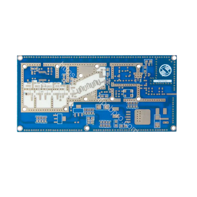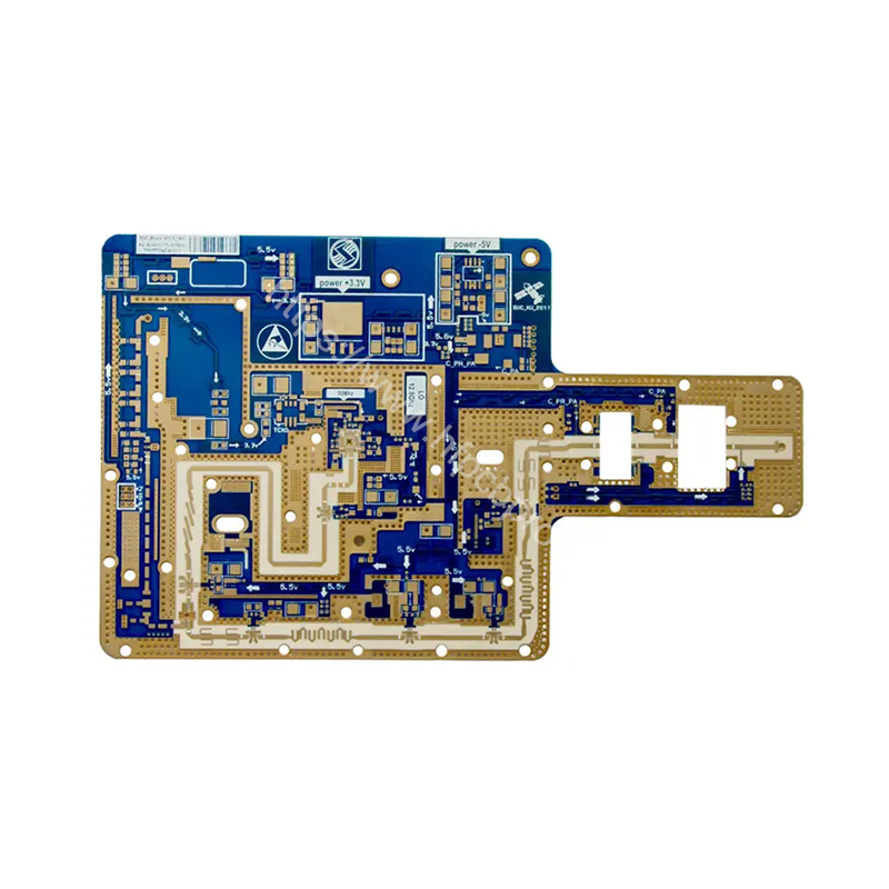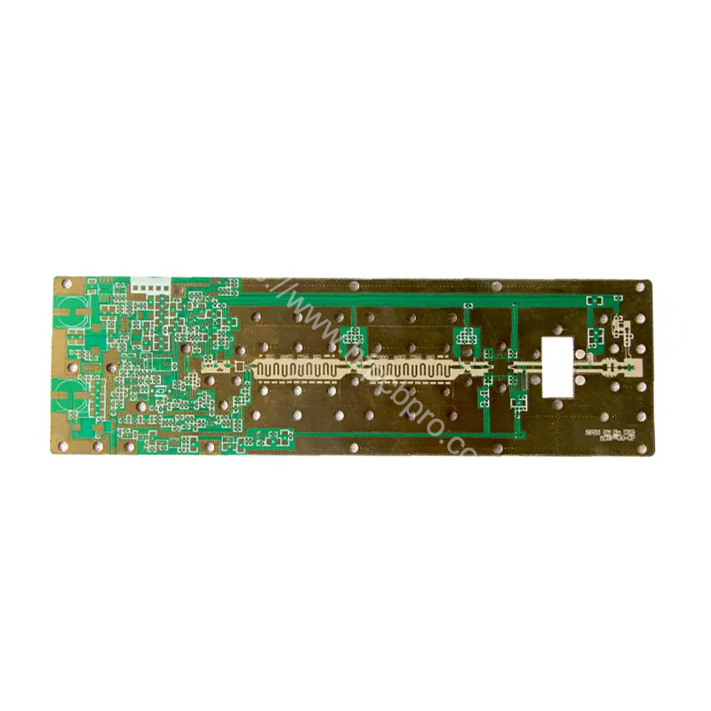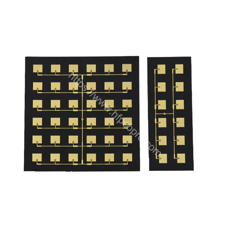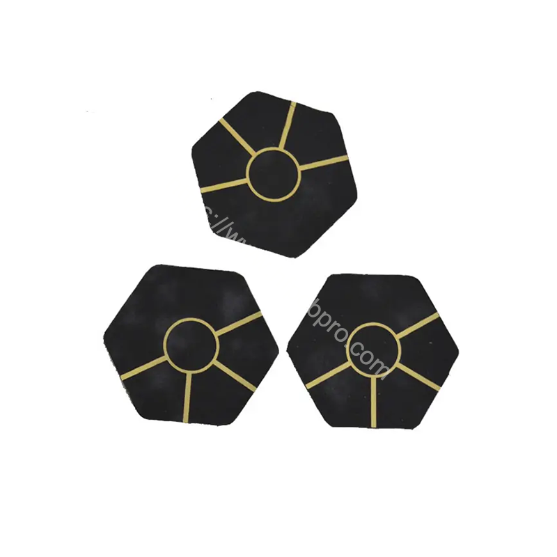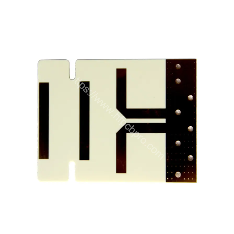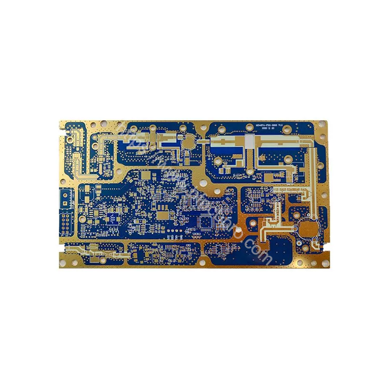
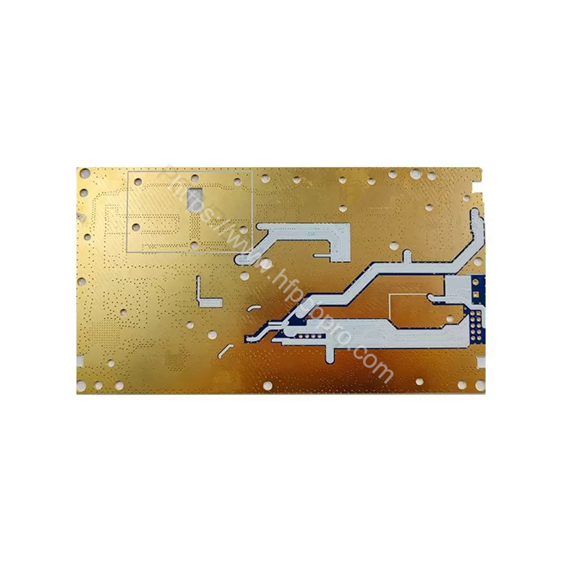
Rogers RO3006 PCB manufacturing for RF and microwave applications using ceramic-filled PTFE laminate. Typical process Dk: 6.15 ± 0.15; Df: 0.0020 at 10 GHz. Send Gerber files, stackup and quantity for a custom PCB fabrication quotation.
| Material | Rogers 4350b |
|---|---|
| Board Thickness | 1.524mm(60mil) |
| Copper Thickness | 1oz/1oz |
| Quanlity Standard | IPC-Ⅱ |
| Dielectric Constant (Dk) | 6.15 @10GHz |
| Dissipation Factor (Df) | 0.0020 @10GHz |
| Surface Finish | ENIG 1u |
Rogers RO3006 PCB fabrication uses a ceramic-filled PTFE laminate with stable electrical properties for compact RF and microwave designs. HF PCB Pro reviews custom RO3006 board stackups, copper specifications, impedance requirements and prototype or production quantities. Send your Gerber files for a manufacturability assessment and quotation.
RO3006 is a ceramic-filled PTFE circuit material from Rogers Corporation. Its dielectric properties are useful for microwave filters, antennas and circuits where a higher dielectric constant can help reduce physical dimensions. The process dielectric constant is not identical to the design dielectric constant, and engineers should select the value appropriate to their modeling method.
| Material property | Typical RO3006 data |
|---|---|
| Laminate family | Ceramic-filled PTFE |
| Process dielectric constant (Dk) | 6.15 ± 0.15 at 10 GHz, 23°C |
| Design dielectric constant | 6.50 (8–40 GHz differential phase length method) |
| Dissipation factor (Df) | 0.0020 at 10 GHz, 23°C |
| CTE in X, Y, Z axes | 17 / 17 / 24 ppm/°C |
| Typical moisture absorption | 0.02% |
Consult the latest Rogers RO3006 laminate documentation for approved material specifications and availability. Actual PCB impedance and insertion loss also depend on construction, copper roughness, transmission-line geometry and processing.
The high dielectric constant of RO3006 can enable compact transmission lines, filters and resonant structures. Its ceramic-filled PTFE formulation offers relatively low dielectric loss and stable performance across a range of temperatures. These characteristics can benefit designs requiring small circuit features and predictable RF behavior. The material does not by itself guarantee a particular insertion-loss figure or operating frequency: simulations and prototype testing remain important.
Compared with conventional FR4, RO3006 offers a specialized dielectric system for microwave work. Compared with lower-Dk Rogers materials such as RO4003C and RO4350B, the higher Dk can change transmission-line width, coupling and circuit dimensions. The ideal choice depends on requirements rather than a single material specification.
A clear fabrication drawing helps the manufacturer evaluate impedance consistency, minimum drill sizes, stackup tolerances and achievable surface finishes. Review our PCB manufacturing capabilities for general fabrication information.
Rogers RO3006 PCB constructions can be considered for RF filters, microwave antennas, compact resonators, wireless communication equipment, satellite electronics and high-frequency test assemblies. Some applications involve demanding radar or mmWave requirements; the final substrate choice should be validated by electrical analysis and measured prototype performance rather than assuming the laminate is qualified for every frequency.
Need to manufacture a Rogers RO3006 PCB? Contact HF PCB Pro for a quotation. Please include your Gerber files, stackup drawing, layer count, laminate thickness, copper weight, surface finish, board dimensions, quantity, impedance targets and desired delivery date. These details help our team assess the construction and respond with a relevant manufacturing proposal.
The published process Dk is 6.15 ± 0.15 at 10 GHz. A separate typical design Dk of 6.50 applies to a specified 8–40 GHz design measurement method. Use the correct value for your transmission-line model.
The published typical Df is 0.0020 at 10 GHz, 23°C. Total insertion loss in a finished PCB also includes conductor and construction effects.
Yes, provided a suitable bonding system and process are selected. A stackup review is especially useful for hybrid constructions and controlled-impedance boards.
We offer a variety of high-frequency materials, including Rogers (e.g., RO4350B, RO5880), Taconic, and PTFE, depending on customer requirements.
Absolutely, we can provide detailed datasheets for review.
Our high-frequency PCBs can support frequencies up to 110 GHz, depending on the design and materials used.
We ensure precise impedance control through accurate stackup design, detailed impedance simulations, and advanced manufacturing processes.
Yes, we can combine materials like FR4 and high-frequency laminates for hybrid PCBs.
Restrictions mainly involve minimum trace width/spacing and material selection, depending on your design requirements.
We enhance thermal performance by using high thermal conductivity materials (e.g., metal-based PCBs) and optimizing copper thickness.
Thermal conductivity ranges from 0.2 W/m·K to 1.0 W/m·K, depending on the material.
ENIG/Gold Plating/Immersion Silver/Silver Plating/HASL/Gold finger/OSP/Nickel-palladium Gold/Resin plugging/Countersinking/ENIG+Hard Gold Plating/ImNi+ImTin/ENIG+OSP
ENIG is recommended due to its flat surface and excellent conductivity for high-frequency use.
We can produce high-frequency PCBs with layers ranging from 2 to 72.
Yes, we specialize in multilayer high-frequency PCBs and support hybrid stackup processes.
The thickness tolerance is ±0.05 mm, and the trace width tolerance is ±10%.
We perform impedance testing, RF performance testing, vacuum thermal testing, and more.
We achieve this by using high-quality materials, optimized manufacturing processes, and strict control of board thickness and other parameters.
Answer: Prototypes typically take 2–7 business days, while mass production takes 6–15 business days, depending on order volume and complexity.
High-frequency materials (e.g., Rogers) are more expensive, and higher layer counts increase complexity and cost.
We ensure reliability by using high-quality materials, rigorous testing, and optimized manufacturing processes.
Yes, our PCBs can endure temperatures up to 260°C and are suitable for harsh environments.
We use anti-static bags, vacuum packaging, and shockproof padding in the outer cartons for protection.
We provide air freight, express delivery, and sea shipping, depending on your needs, DHL is always prefered that ensure timely delivery through reliable logistics.