
Parameters of Rogers RT/duroid® 5880 High-Frequency Laminate

Parameters of Rogers RT/duroid® 5880 High-Frequency Laminate Dk 2.20 ± 0.02, Df 0.0009, 0.02% moisture absorption — the measured parameters, key features and applications behind PTFE’s lowest-loss laminate. Table of Contents RT/duroid 5880 high-frequency laminate is a polytetrafluoroethylene (PTFE) glass fiber-reinforced material. The microfibers within the board are randomly distributed, providing maximum strength enhancement for […]
Key Considerations for High-Frequency PCB Design and Fabrication
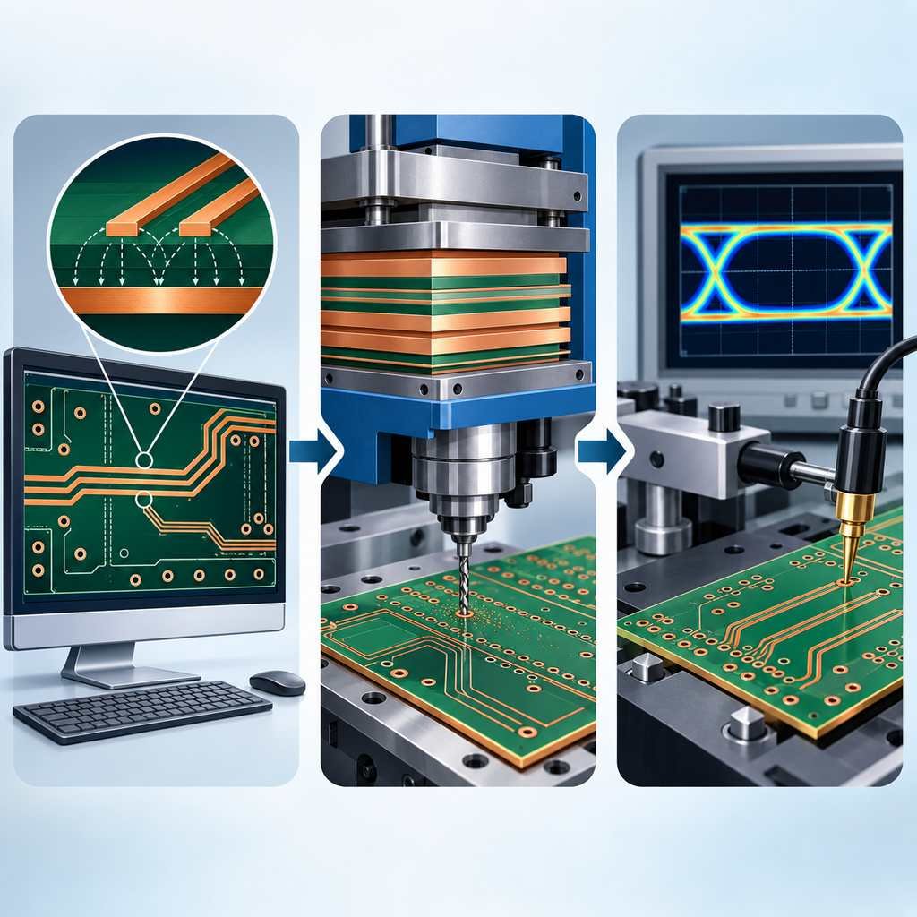
Key Considerations for High-Frequency PCB Design and Fabrication From Dk < 3.5 material selection to TDR verification — the design rules, process windows and test gates that keep GHz-level boards inside spec. Table of Contents High-frequency PCB performance is decided across three phases: design, fabrication, and testing. This guide walks through the material, impedance, stack-up, […]
ENIG, Plated Gold, DIG, Thick Gold, Thin Gold—What’s the Difference?
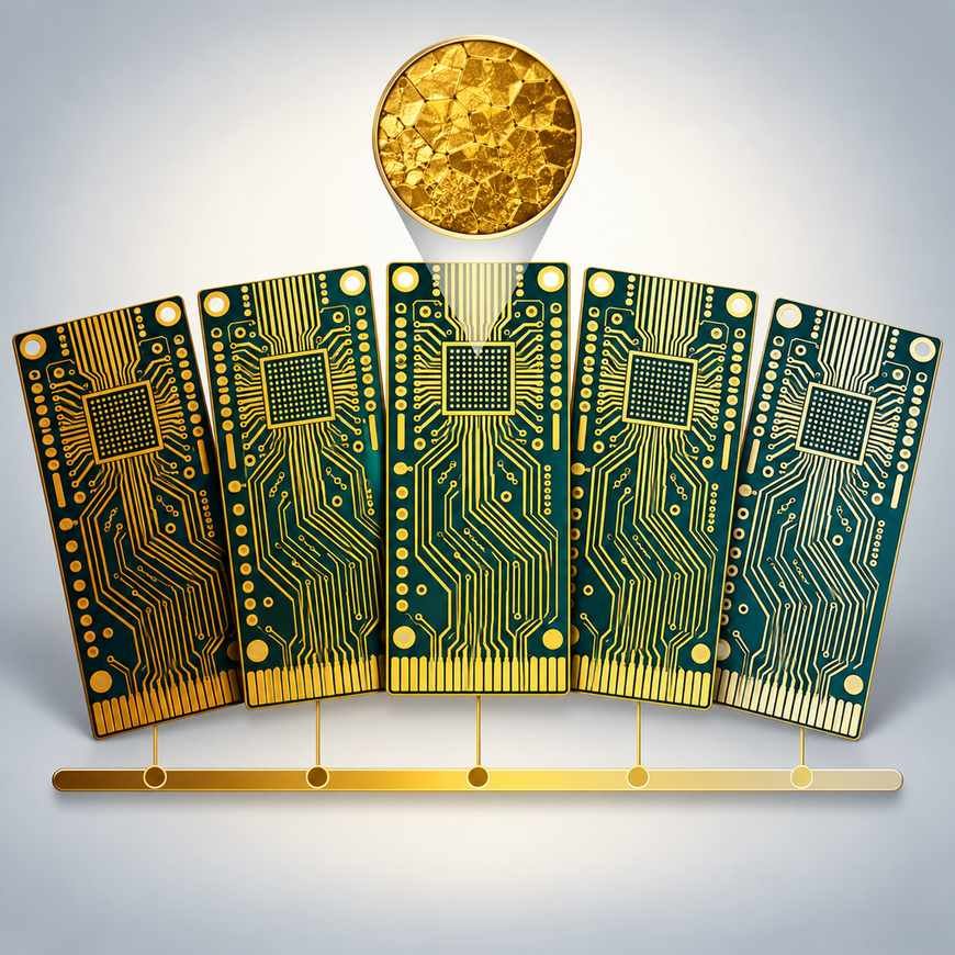
ENIG, Plated Gold, DIG, Thick Gold, Thin Gold—What’s the Difference? Every gold surface finish decoded — structure, RF loss, solderability and bondability — so you never pick the wrong finish for a high-frequency board. Table of Contents Gold surface finishes can be extremely confusing: ENIG, plating gold, nickel-gold, immersion gold, thick gold, thin gold, palladium-gold, […]
High frequency PCB circuit board
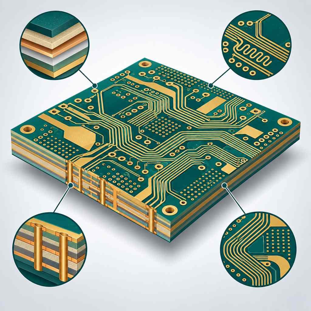
High Frequency PCB Circuit Board What a high-frequency PCB circuit board is, the substrates and layout rules behind it, how it is manufactured — and where the technology is heading next. Table of Contents High-frequency PCB circuit boards are a crucial component in the electronics industry, specifically designed for high-frequency signal transmission with excellent electrical […]
Steps and Considerations for Impedance Control in High-Frequency PCB Manufacturing
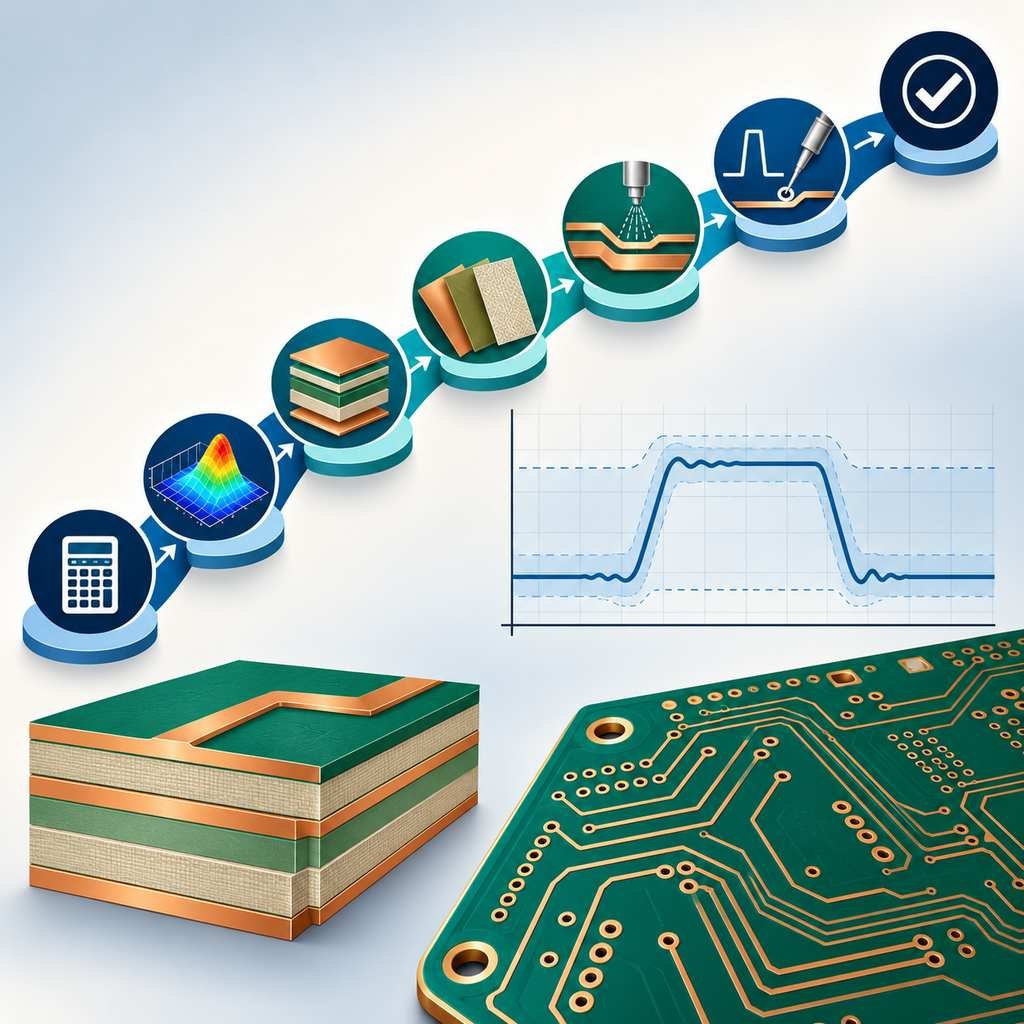
Steps and Considerations for Impedance Control in High-Frequency PCB Manufacturing From design calculation and simulation to TDR verification — the seven steps and five disciplines that keep impedance inside tolerance on high-frequency PCBs. Table of Contents Impedance control is crucial for signal integrity and circuit performance in high-frequency PCBs, especially in applications involving RF, microwave, […]
Finished Product Testing and Environmental Simulation Equipment in the Production Process of High-Frequency PCBs
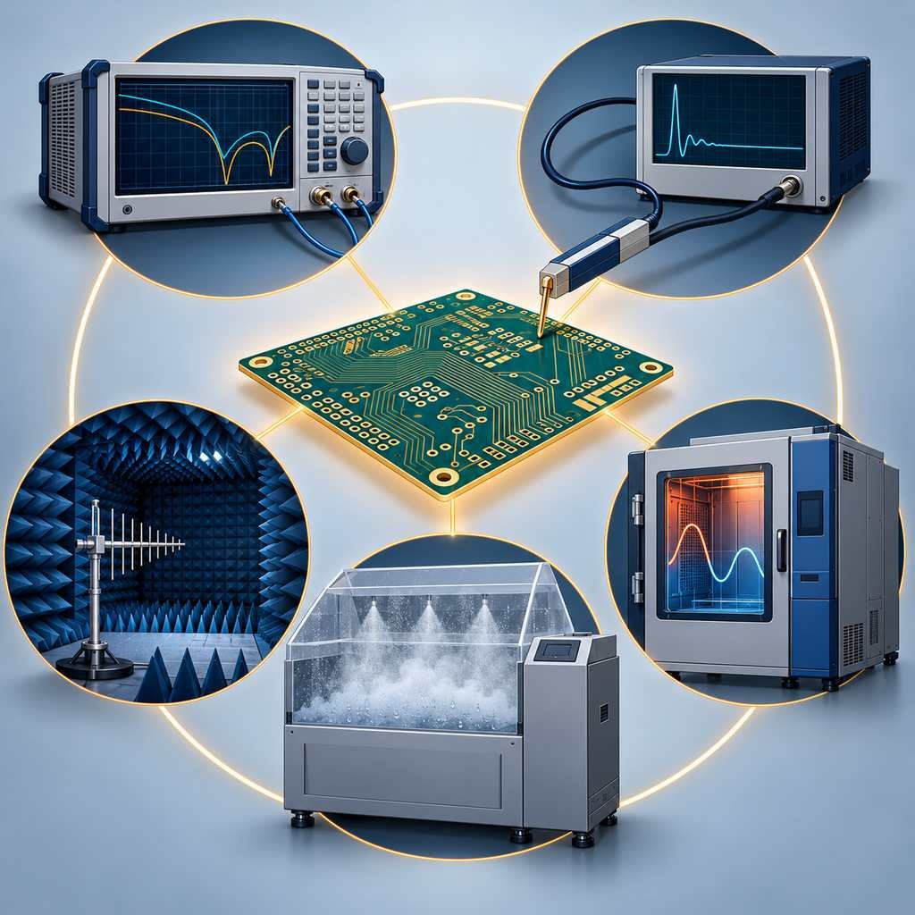
Finished Product Testing and Environmental Simulation Equipment in the High-Frequency PCB Factory Network analyzers, TDR, thermal cycling, salt fog and EMI chambers — the test and environmental simulation equipment that guarantees high-frequency PCB reliability. Table of Contents With the rapid development of fields such as high-frequency communication, 5G, satellite navigation, and radar technology, the application […]
Post-Processing Steps and Considerations in High-Frequency PCB Production
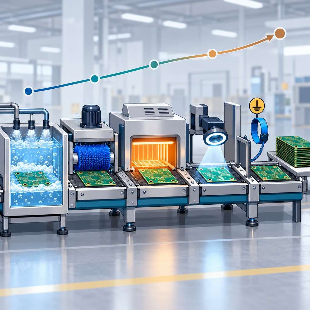
Post-Processing Steps and Considerations in High-Frequency PCB Production Cleaning, deburring, drying, inspection and ESD control — the post-processing steps, common failure modes and emerging trends behind reliable high-frequency PCBs. Table of Contents Post-processing is the final gate of high-frequency PCB production: the cleaning, finishing and inspection steps that happen after plating, etching and soldering. Done […]
High-Frequency PCB Production: Steps and Considerations for Microstrip and Stripline Design
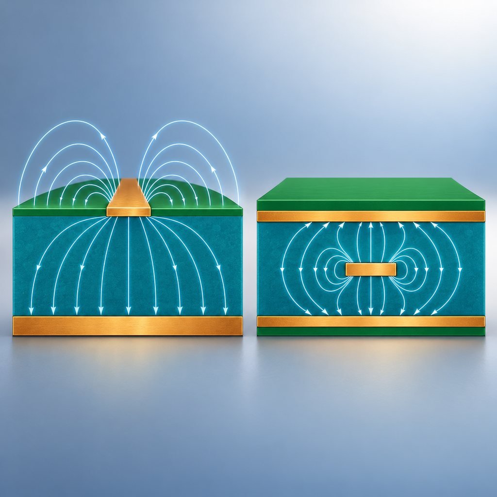
High-Frequency PCB Production: Steps and Considerations for Microstrip and Stripline Design From impedance targets and substrate selection to simulation, tolerances, and the four most common failure modes — a practical walkthrough of microstrip and stripline design in high-frequency PCB production. Table of Contents Basic Concepts of Microstrip and Stripline Microstrip: A widely used transmission line […]
Steps and Considerations for Surface Treatment in High-Frequency PCB Production
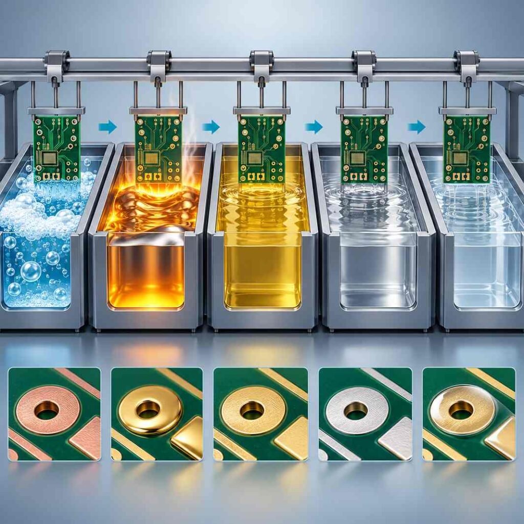
Steps and Considerations for Surface Treatment in High-Frequency PCB Production The five process steps from cleaning to testing, key control points, and an honest comparison of HASL, ENIG, tin, silver and coating treatments — plus fixes for the four most common plating defects. Table of Contents Main Steps in Surface Treatment Surface treatment directly affects […]
Laser Engraving and Marking Equipment in High-Frequency PCB Manufacturing
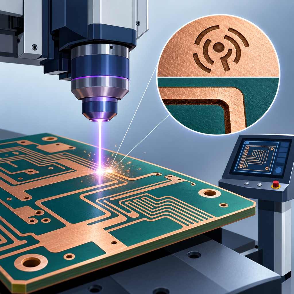
Laser Engraving and Marking Equipment in High-Frequency PCB Manufacturing How laser engraving and marking works, where it fits in high-frequency PCB production — pad engraving, trace cutting, traceability marking — and the five advantages that make it indispensable. Table of Contents Overview of Laser Engraving and Marking Equipment Laser engraving and marking equipment directs a […]
Optical Microscopes and Electron Microscopes in High-Frequency PCB Manufacturing
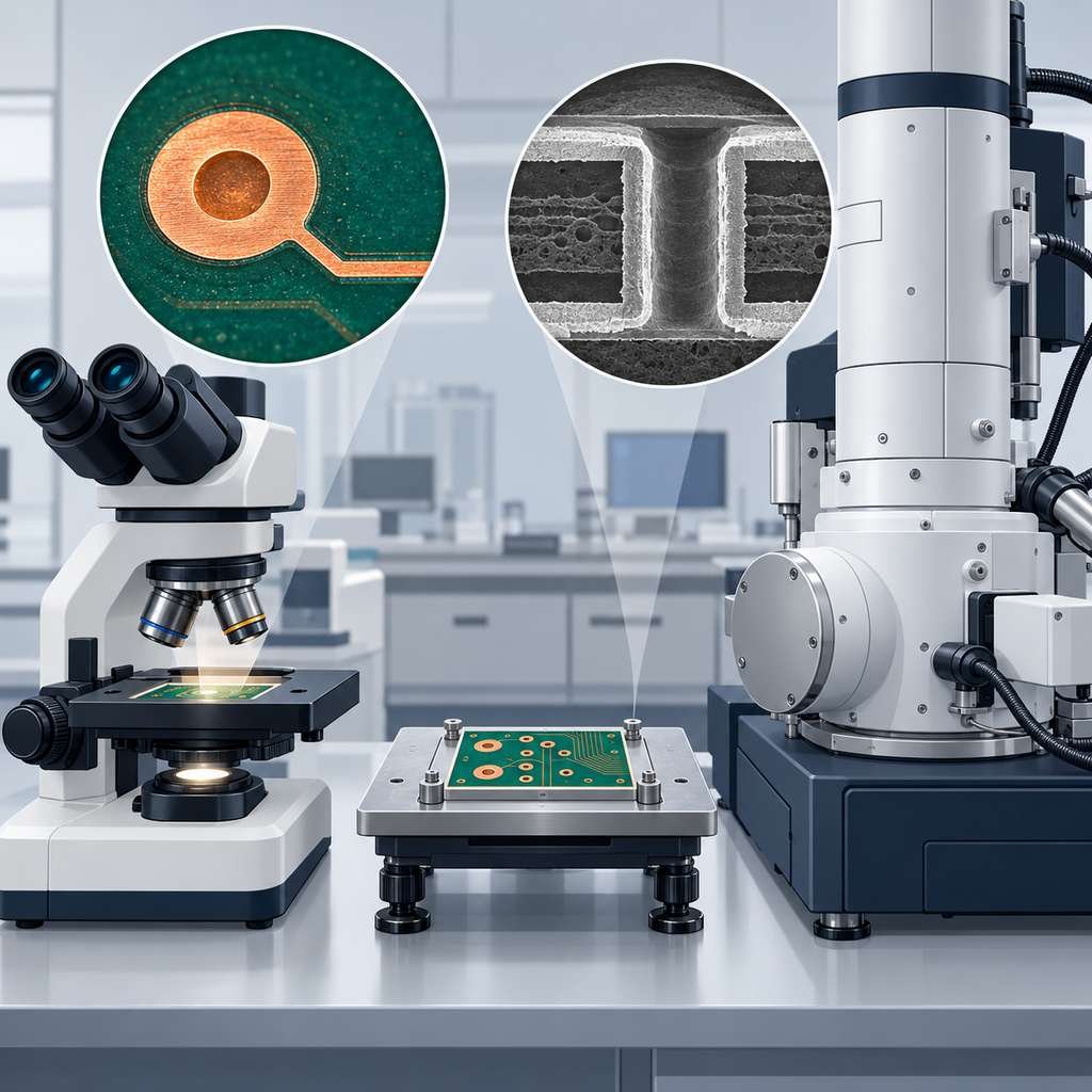
Optical Microscopes and Electron Microscopes in High-Frequency PCB Manufacturing Working principles, five application areas from BGA inspection to micro-via analysis, and when each microscope technology earns its place on the production floor. Table of Contents Overview: Optical Microscopes vs Electron Microscopes Optical microscopes magnify objects with an optical lens system using visible light. They are […]
Laser Etching Machine in High-Frequency PCB Production Process
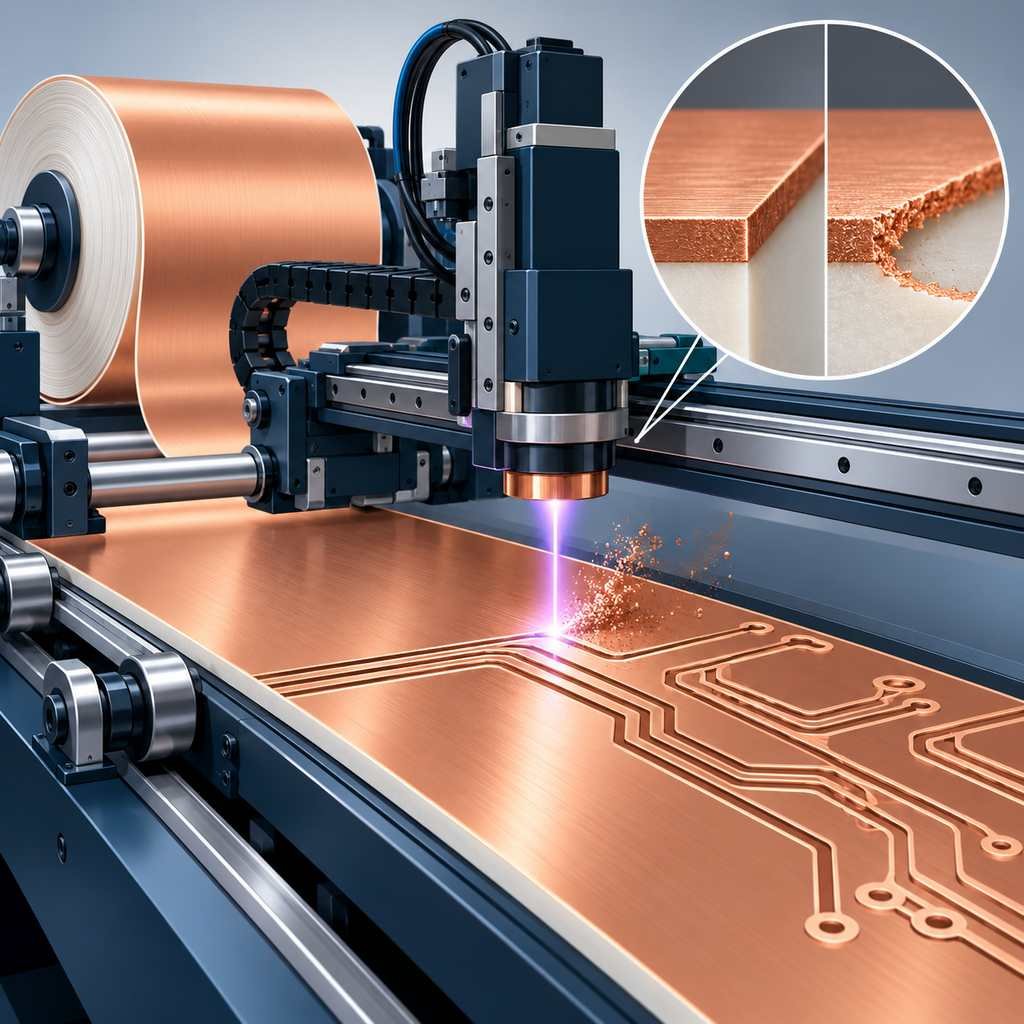
Laser Etching Machine in High-Frequency PCB Production Process How laser etching machines form circuit patterns on PTFE, ceramic and polyimide laminates — working principles, five applications, and why they outperform chemical etching for high-frequency work. Table of Contents Overview of Laser Etching Machines In high-frequency PCB production, etching is the step that forms the circuit […]