High-Frequency PCB Insights & Resources

Technical guides, material comparisons and process insights on high-frequency, RF and microwave PCB manufacturing.

RT/duroid 5880 PTFE laminate panel with gauges for its electrical parameters and a nearly flat low-loss curve

Parameters of Rogers RT/duroid® 5880 High-Frequency Laminate

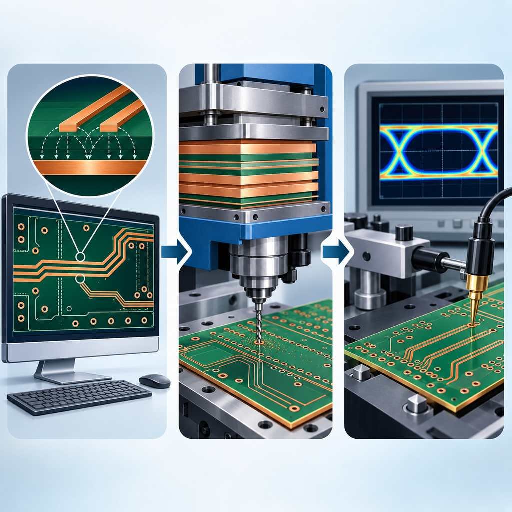
High-frequency PCB design, fabrication and test stages linked in sequence, from layout to lamination and drilling to probe verification

Key Considerations for High-Frequency PCB Design and Fabrication

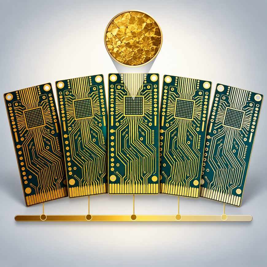
Five high-frequency PCB coupons comparing different gold surface finishes with a magnified grain texture

ENIG, Plated Gold, DIG, Thick Gold, Thin Gold—What’s the Difference?

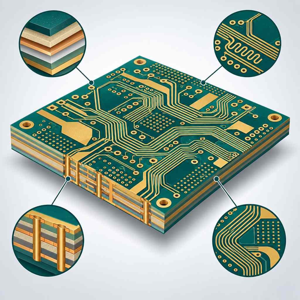
High-frequency circuit board with callouts for substrate selection, impedance layout rules, precision fabrication and future technology

High frequency PCB circuit board

Seven-step impedance control flow for high-frequency PCB manufacturing beside a pulse sitting inside its tolerance band

Steps and Considerations for Impedance Control in High-Frequency PCB Manufacturing

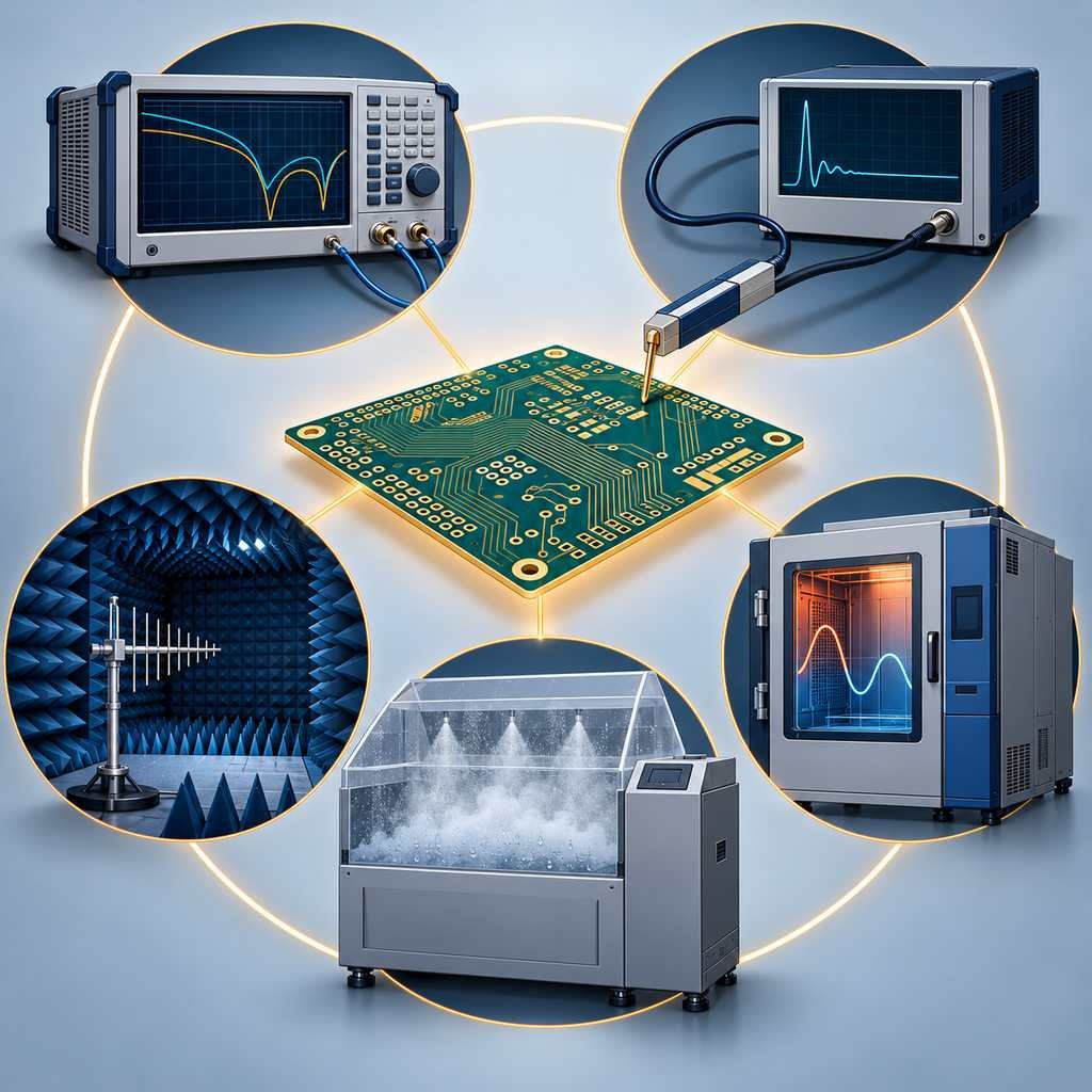
Five high-frequency PCB test and environmental simulation instruments arranged around a circuit board

Finished Product Testing and Environmental Simulation Equipment in the Production Process of High-Frequency PCBs

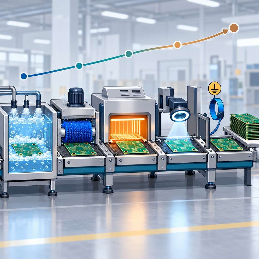
Five high-frequency PCB post-processing stations along a conveyor, from cleaning and deburring through drying, inspection and ESD control

Post-Processing Steps and Considerations in High-Frequency PCB Production

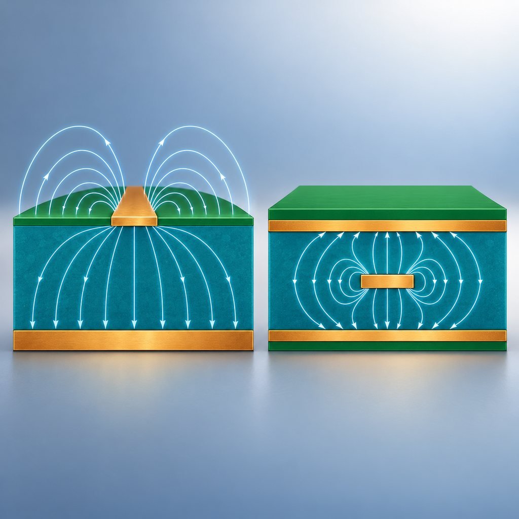
Microstrip and stripline PCB cross-sections side by side showing their different field patterns and reference planes

High-Frequency PCB Production: Steps and Considerations for Microstrip and Stripline Design

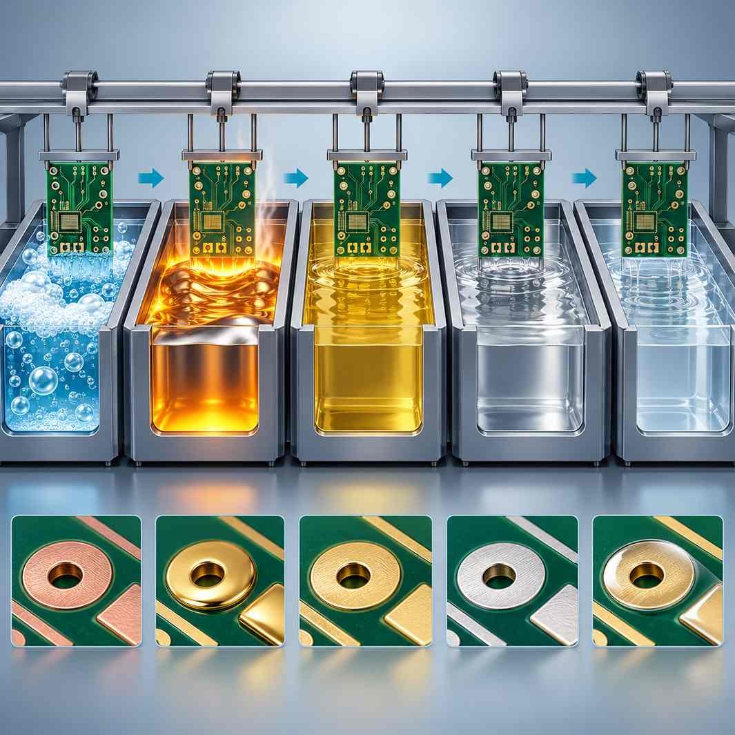
Five high-frequency PCB surface treatment tanks in sequence with five finished pad finishes compared below

Steps and Considerations for Surface Treatment in High-Frequency PCB Production

Laser engraving and marking head cutting trace patterns and traceability marks onto a high-frequency PCB

Laser Engraving and Marking Equipment in High-Frequency PCB Manufacturing

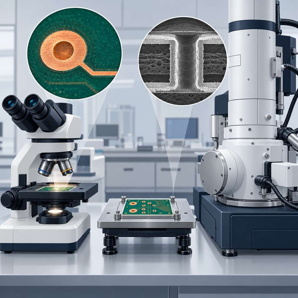
Optical microscope and electron microscope side by side with magnified BGA joint and micro-via cross-section views

Optical Microscopes and Electron Microscopes in High-Frequency PCB Manufacturing

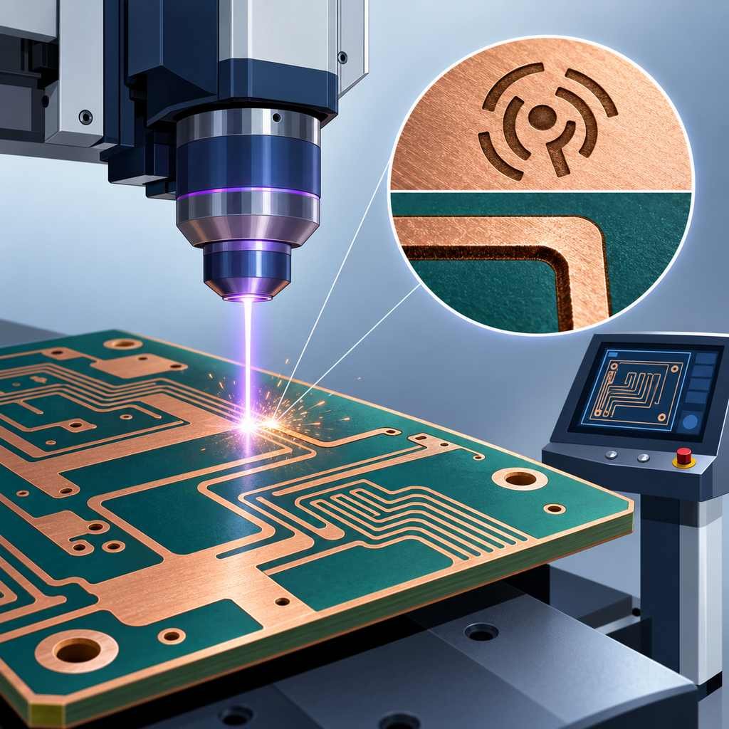
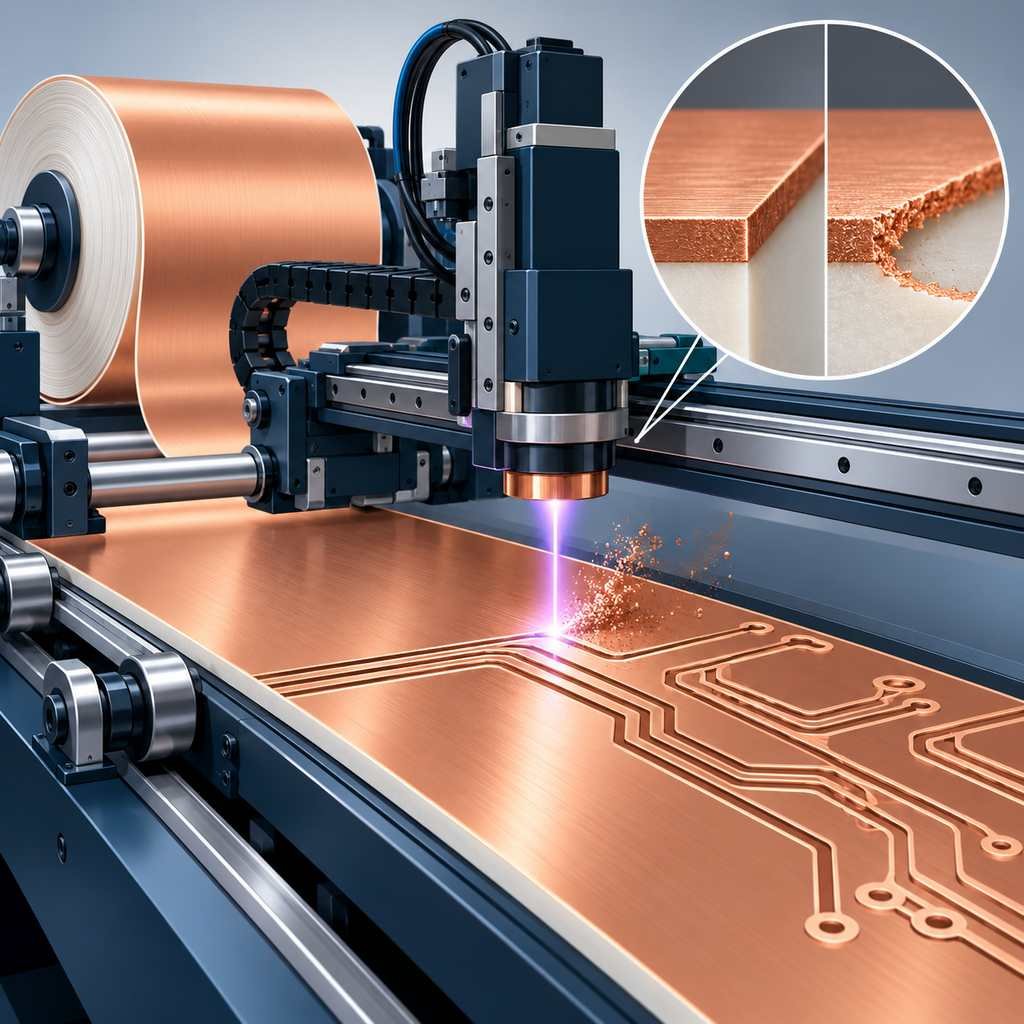
Laser etching machine cutting circuit patterns into a PTFE laminate with a magnified comparison of laser and chemical trace edges

Laser Etching Machine in High-Frequency PCB Production Process

PCB Assembly

PCBA Services

Quality

Application

Resources

Printed Circuit Board

RF PCB

Quality

PCB Surface Finish

Printed Circuit Board

Drills & Throughplating

Profiles

PCB Stackup

Resources