High-Frequency PCB Insights & Resources

Technical guides, material comparisons and process insights on high-frequency, RF and microwave PCB manufacturing.

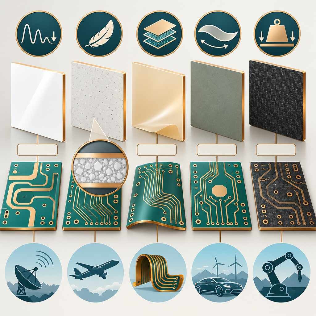
Five high-frequency substrate families as sample tiles from PTFE through ceramic-filled, flexible LCP, modified PPE and special composites

Five Key Materials Shaping the Performance Cornerstone of Modern Electronic Equipment

Four high-frequency PCB pad coupons comparing ENIG, soft gold, immersion silver and OSP finishes with magnified grain and finish job icons

Winning by a Hair’s Breadth: Analyzing the Choices and Profound Impact of Surface Finish Processes in High-Frequency PCBs

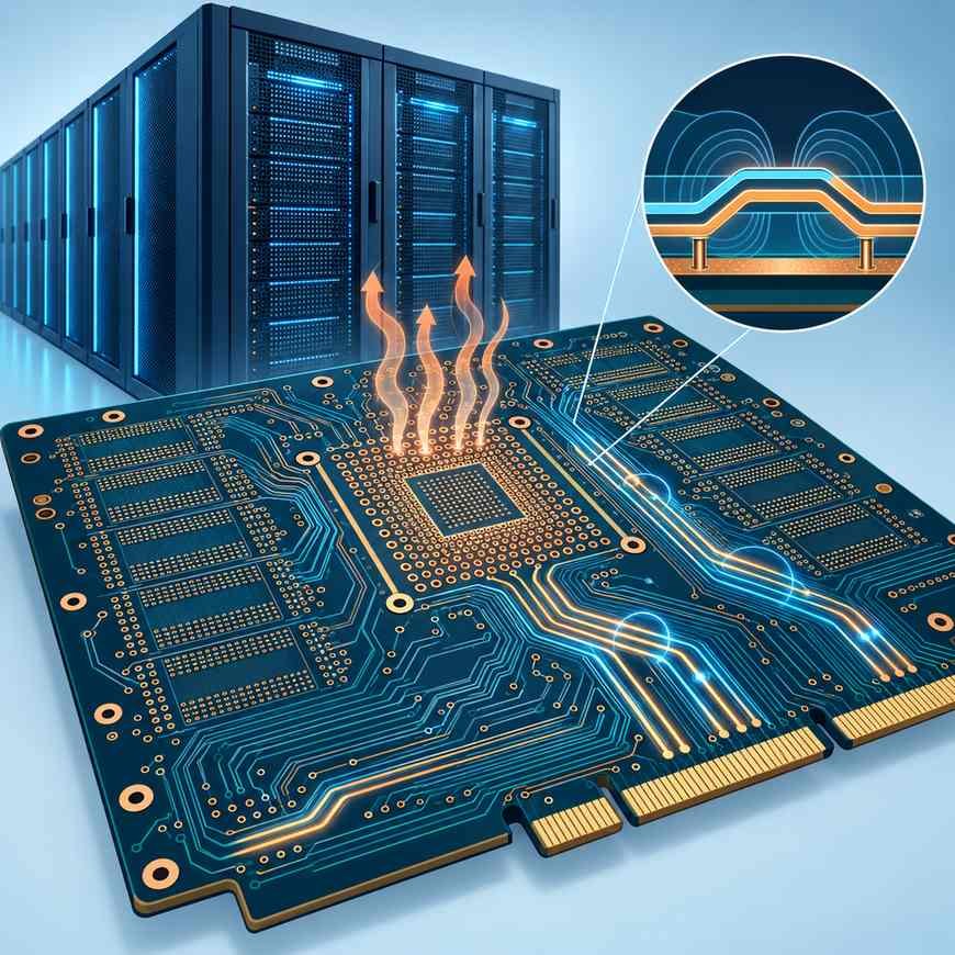
AI server rack behind a high-frequency board with a GPU package, memory modules, low-loss channels and a magnified differential pair

At the Summit of the AI Wave: High-Frequency PCBs – The Invisible Foundation of Computing Power

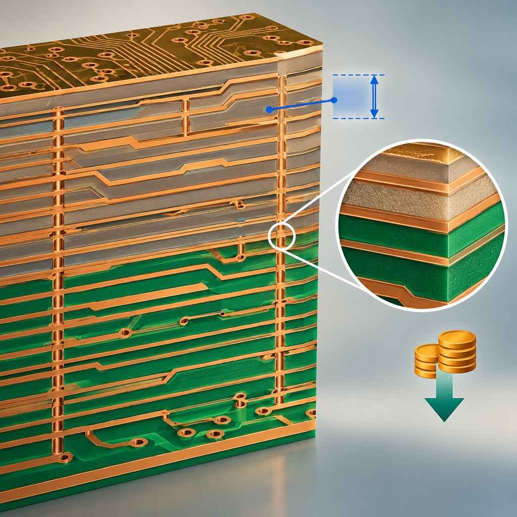
Tall hybrid multilayer stack bonding high-frequency and FR-4 layers with a tight impedance bracket and a reduced cost tag

Pushing Technical Boundaries: Exceptional Properties and Application Value of Rogers FR Multilayer Laminated High-Frequency Circuit Boards

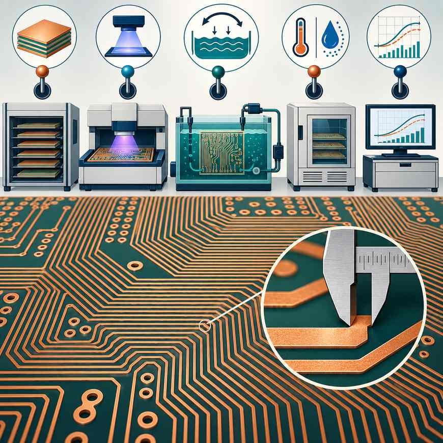
Five control levers for micron line width tolerance above a dense fine-line trace pattern with a magnified caliper measurement

How Microwave PCB Manufacturers Achieve ±0.02mm Line Width Tolerance

RT/duroid 5880 board at the centre of three concentric property rings covering dielectric stability, loss, moisture, reach, reliability and manufacturability

Analysis of the Exceptional Properties and Core Advantages of Rogers 5880 High-Frequency Circuit Boards

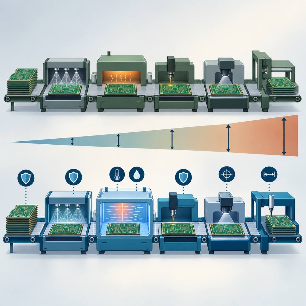
Parallel standard and high-frequency PCB production lines with a widening gap between them and added climate and tolerance controls

Key Differences Between High-Frequency Circuit Board and Standard Circuit Board Manufacturing Processes

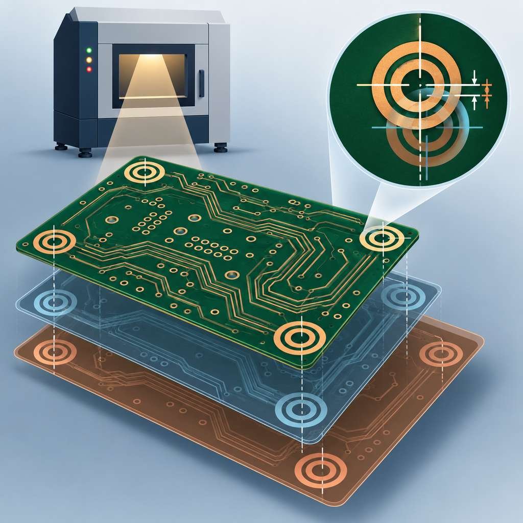
Multilayer PCB with concentric X-ray registration targets showing inner layer offset, examined by an X-ray inspection cabinet

Professional Circuit Board Manufacturer Xincheng’er Electronics Analyzes the Causes of PCB Layer Misalignment

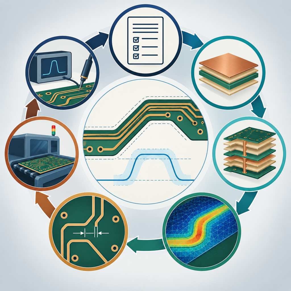
Seven-step controlled impedance design ring from requirement and material through simulation, routing, factory control and TDR verification

English: How to Design a PCB with Controlled Impedance in High-Frequency Applications

Eight high-frequency PCB test categories arranged around a board, from TDR impedance and signal integrity to thermal, mechanical and reliability testing

Key Points to Consider During High-Frequency PCB Testing

Rising high-frequency PCB development curve with four trend markers above and four challenge barriers below

Development Trends and Challenges of High-Frequency PCBs

Seven electrical and physical selection indicators ringed around a laminate panel with a criteria checklist

Key Electrical Indicators for Selecting High-Frequency PCB Materials

PCB Assembly

PCBA Services

Quality

Application

Resources

Printed Circuit Board

RF PCB

Quality

PCB Surface Finish

Printed Circuit Board

Drills & Throughplating

Profiles

PCB Stackup

Resources