PTFE–FR-4 hybrid constructions explained: lamination stress, PTFE drilling, plasma activation, copper adhesion and layer registration — with the process controls that make them manufacturable.
High frequency hybrid PCB technology has become a critical foundation for modern 5G communication systems, millimeter-wave radar, satellite communication equipment, aerospace electronics and advanced RF testing devices. By combining low-loss RF materials — such as Rogers RO4000 series and Taconic PTFE laminates — with conventional FR-4 in a single multilayer stack-up, manufacturers get both excellent signal integrity and cost-effective mechanical stability.
But building this kind of board is far more complicated than standard multilayer fabrication. Different material characteristics, thermal expansion mismatches, drilling instability, copper adhesion issues and dimensional control all create serious production challenges.
This article walks through the key manufacturing difficulties of high frequency hybrid PCBs and the advanced engineering solutions leading PCB manufacturers use to solve them.
Hybrid constructions earn their place wherever a design needs stable RF performance and low transmission loss above 1 GHz — without paying full PTFE pricing for layers that do not carry RF signals. Compared with fully PTFE-based circuit boards, a high frequency PCB built as a hybrid stack cuts production cost significantly while keeping the electrical performance that matters.
Typical applications include:
Because these systems operate at extremely high frequencies, even small manufacturing defects land directly on insertion loss, impedance consistency and signal reliability.
The biggest challenge in hybrid PCB manufacturing comes from the physical differences between PTFE-based RF materials and FR-4 substrates — two material families that were never designed to be pressed together.
FR-4 has a Z-axis coefficient of thermal expansion (CTE) of around 50–70 ppm/°C, while PTFE materials may reach 200–300 ppm/°C. During lamination and soldering, this thermal expansion mismatch generates strong internal stress, and manufacturers run into delamination, board warpage, blistering, resin cracking and via reliability failures.
PTFE is chemically inert and naturally resists adhesion — that is part of what makes it such a good RF dielectric and such a difficult laminating partner. Its soft surface structure produces weak bonding strength when combined with FR-4 layers.
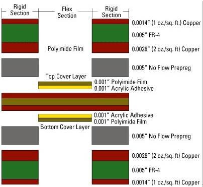
Modern PCB factories solve these problems through tightly controlled lamination processes — the fix is less about one magic material and more about three disciplines working together.
Low-flow adhesive prepregs are commonly used between RF materials and FR-4 layers. These bonding films absorb the stress between dissimilar laminates while improving interface adhesion.
Rather than one simple press cycle, manufacturers use gradual temperature ramping and segmented pressure control to stabilize resin flow and reduce stress concentration. Key process improvements include:
Engineers often place RF layers symmetrically within the PCB stack-up to minimize warpage during thermal cycling — an unbalanced construction will visibly bow as it moves through reflow.
Drilling hybrid PCBs is significantly harder than drilling standard FR-4. PTFE is soft and elastic while glass-reinforced FR-4 is abrasive and rigid — so the bit sees two completely different materials in one hole, which destabilizes it at high spindle speeds.
Common defects include:
PTFE adds one more trap: an “elastic memory” effect, where the material partially recovers after drilling, pulling hole dimensions out of spec.
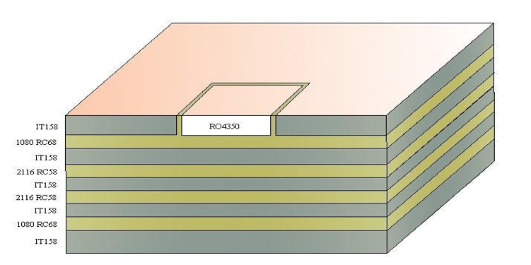
To keep via reliability and hole accuracy on target, advanced fabs optimize the drilling process from three angles.
Diamond-coated or ultra-hard carbide drills improve cutting stability and resist the wear that fiberglass reinforcement causes on standard bits.
Factories typically run high spindle speed with low feed rate, multiple peck drilling cycles and controlled heat generation — the combination that keeps PTFE’s elasticity from deforming the hole.
Aluminum entry sheets and composite backup boards stabilize drilling quality while reducing exit burrs and deformation at both faces of the panel.
Copper plating reliability is considered the most critical process in high frequency hybrid PCB fabrication. PTFE surfaces are naturally hydrophobic and chemically inert, which makes direct copper adhesion extremely difficult.
Without proper treatment, the board may suffer from:
Traditional desmear processes simply do not work on PTFE, so advanced surface activation is required before metallization.
Plasma treatment has become the industry-standard solution for PTFE activation. Using CF4/O2 plasma gas mixtures, manufacturers create microscopic anchor structures on the PTFE surface while raising its surface energy. The benefits:
Pulse electroplating ensures uniform copper thickness inside complex via structures and across hybrid material interfaces, and it measurably improves current carrying capacity, thermal reliability, signal integrity and via consistency.
At millimeter-wave frequencies, transmission line geometry has to be extremely precise — and PTFE materials move during lamination, drilling, chemical processing and thermal cycling.
The result is serious layer alignment challenges, because even tiny registration errors affect:
Fabs answer dimensional drift with three complementary measures.
Manufacturers use historical shrinkage data to pre-compensate artwork dimensions before imaging, so each material’s known movement is corrected in advance rather than discovered after the press.
LDI eliminates film distortion from the imaging process and improves registration accuracy to within ±15 µm — a level conventional film exposure cannot hold on moving materials.
Where the design allows it, ceramic-filled laminates such as Rogers RO4350B offer much better dimensional stability than pure PTFE — material selection itself is a registration-control decision.
Reliable RF production does not end after fabrication — strict inspection and reliability validation are what prove the board will survive the field. Three test families cover it.
Modern factories combine X-ray inspection, ultrasonic scanning microscopy, AOI and cross-section analysis to catch internal defects without destroying the panel.
Vector network analyzers measure insertion loss, return loss, signal attenuation and impedance consistency against the design targets.
Common reliability tests include 288 °C solder float testing, thermal shock cycling, peel strength testing and IST testing — the passes that predict how the board handles assembly and years of operation.

High frequency hybrid PCB manufacturing is one of the most demanding processes in the electronics industry. Combining PTFE RF materials with conventional FR-4 successfully takes deep expertise in material science, precision drilling, plasma surface treatment, multilayer lamination and dimensional control.
As 5G infrastructure, autonomous driving, satellite communication and millimeter-wave technologies keep growing, demand for reliable hybrid boards will grow with them. Manufacturers that master these advanced fabrication techniques — and the ones above in particular — will hold a decisive edge in the future of wireless communication and high-speed electronic systems.
Common questions about high-frequency hybrid (mixed-dielectric) PCB manufacturing.
A multilayer circuit board that combines RF materials such as PTFE laminates with standard FR-4 in one stack-up — the RF layers get the low-loss dielectric they need while the rest of the board keeps FR-4's cost and mechanical stability.
PTFE has low surface energy, poor adhesion characteristics and a high thermal expansion rate, which makes drilling, plating and lamination considerably more complicated than standard FR-4 processing.
Plasma treatment roughens the PTFE surface and raises its surface energy so copper can bond reliably to the hole walls — without it, plating failures show up under thermal stress.
5G communication, aerospace, automotive radar, satellite communication, RF test equipment and microwave electronics all rely on hybrid constructions for their balance of RF performance and cost.
Maintaining reliable copper adhesion and dimensional stability while combining materials with completely different thermal and mechanical behavior — nearly every process decision serves that goal.
Send us your stack-up and material combination. Our engineering team will review the lamination plan, drilling and plating strategy, then quote your hybrid RF board.
Get An Engineering Review → Fast Reply on WhatsApp