Dk, Df, thermal stability, and moisture resistance explained — plus the major laminate families and design rules behind reliable 5G, radar, and high-speed boards.
High-frequency PCB technology plays a critical role in modern wireless communication, radar systems, satellite electronics, and high-speed data transmission. As operating frequencies rise beyond 1 GHz, conventional FR-4 is no longer sufficient for maintaining signal integrity, minimizing transmission loss, and ensuring stable electrical performance.
High-frequency PCBs are specially engineered to transmit RF, microwave, and millimeter-wave signals with minimal attenuation. They are widely used in 5G base stations, automotive radar, aerospace systems, Wi-Fi 6/7 devices, and high-speed networking equipment.
Compared with standard PCB materials, high-frequency laminates offer lower dielectric constant (Dk), lower dielectric loss (Df), superior thermal stability, and better impedance consistency. Choosing the right material and optimizing the stack-up are essential for reliable performance in demanding RF applications.
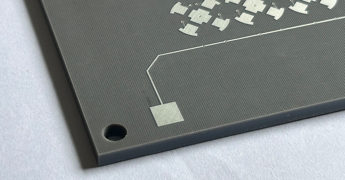
Low dielectric constant (Dk). Dk determines how quickly signals travel through the substrate — lower Dk means faster propagation and less delay. Typical ranges:
Low dielectric loss (Df). Df measures how much signal energy dissipates as heat — lower Df means lower insertion loss and better signal quality over long paths:
Thermal stability and mechanical reliability. Materials must survive thermal cycling while staying dimensionally and electrically consistent — look for low CTE, high Tg, strong copper peel strength, and good rigidity. These prevent delamination, warpage, and impedance drift during fabrication and long-term operation.
Moisture resistance. Absorbed moisture shifts dielectric properties at high frequencies. LCP and PTFE absorb extremely little water, which is what makes them suitable for harsh outdoor and aerospace environments.
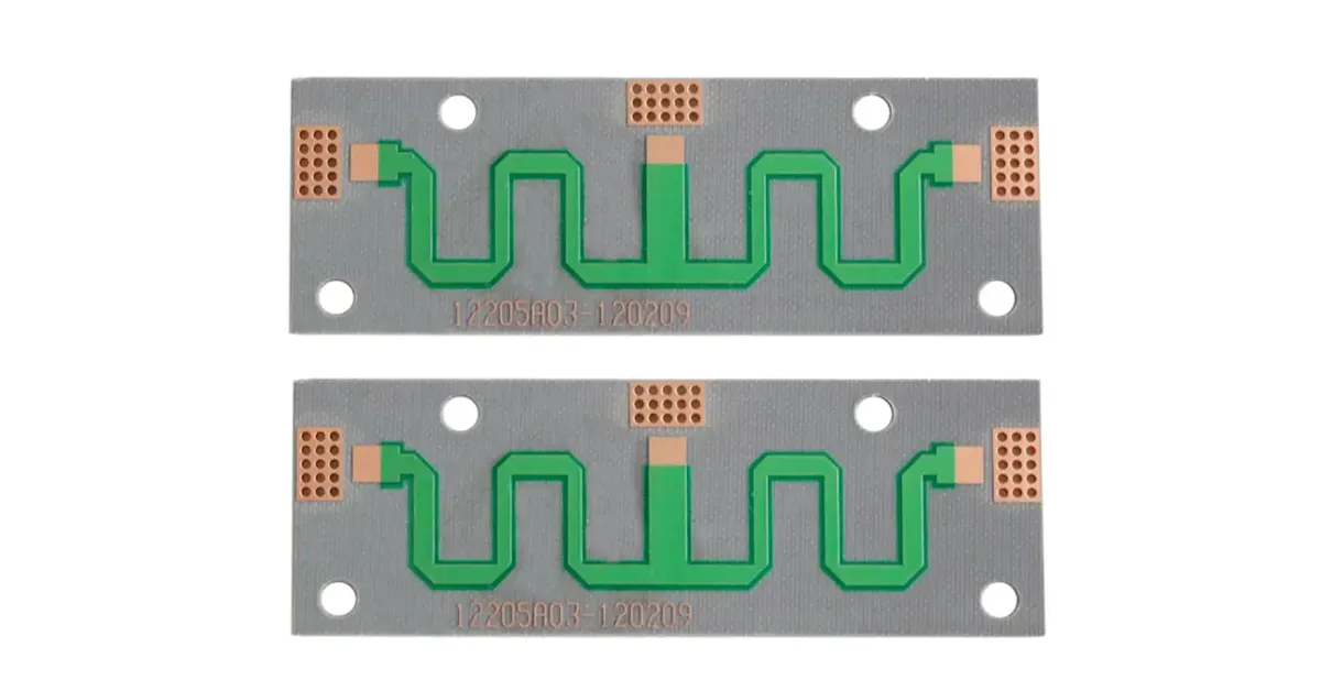
PTFE-based materials set the benchmark for ultra-low loss and excellent RF performance — Rogers RT/duroid and Taconic RF laminates are the classics, used in millimeter-wave radar, aerospace communication, satellite antennas, and precision RF test equipment. For the PTFE classics, see our RT/duroid 5870 & 5880 guide.
Hydrocarbon ceramic laminates combine good RF performance with easier processing than PTFE — Rogers RO4350B and RO4003C lead this family, alongside Panasonic Megtron. Typical uses: automotive radar, RF power amplifiers, base station antennas, and microwave modules.
Modified epoxy materials offer a cost-effective option for medium-frequency applications while keeping full compatibility with standard FR-4 manufacturing — Wi-Fi modules, Bluetooth devices, consumer electronics, and industrial IoT.
Liquid crystal polymer (LCP) brings extremely low moisture absorption, natural flexibility, and stable high-frequency performance — ideal for flexible RF circuits, wearables, compact antenna modules, and high-frequency flex interconnects.
Ceramic-filled laminates provide higher dielectric constants, better thermal conductivity, and superior miniaturization — commonly found in RF filters, couplers, and high-power microwave systems.
For brand-level availability across all these families, see our high-frequency PCB materials inventory.
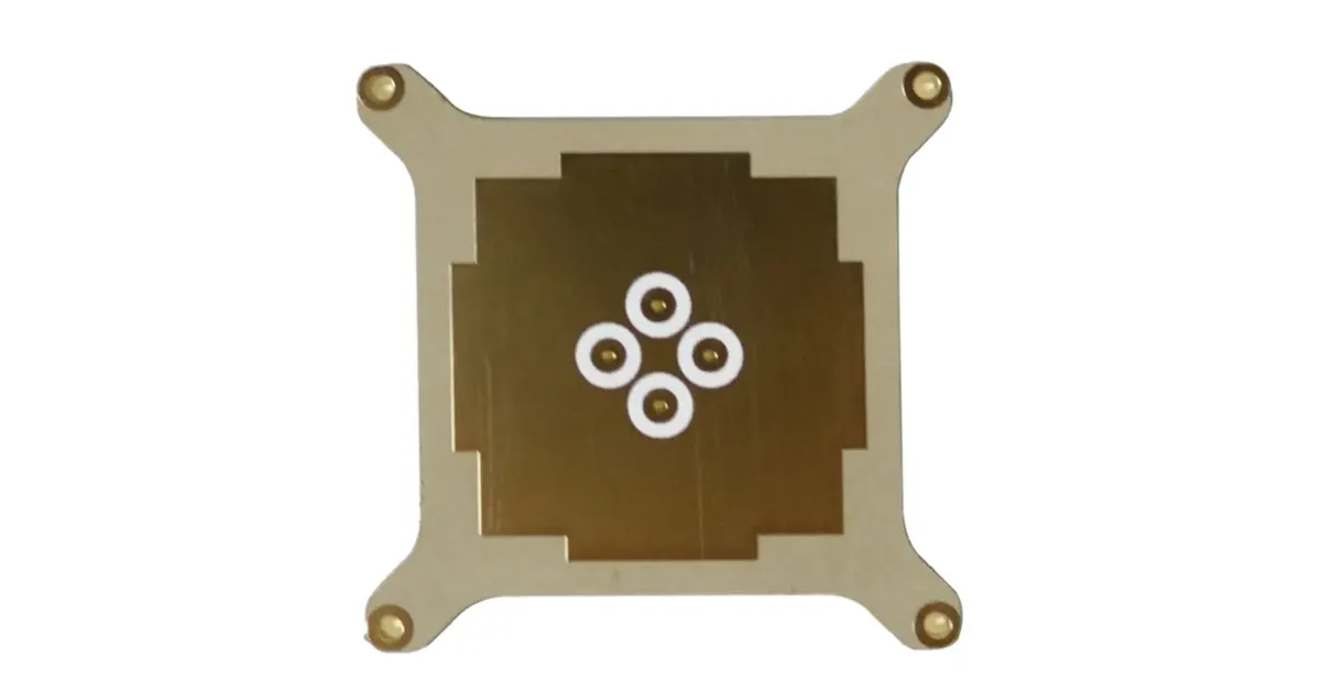
Controlled impedance design. Even small impedance deviations cause reflections and insertion loss. Engineers typically simulate trace width, spacing, and dielectric requirements in tools such as ADS, HyperLynx, or HFSS before committing to a stack-up.
Routing optimization. Keep traces short and straight, minimize via count, use blind or buried vias where appropriate, and maintain consistent differential pair spacing — especially in high-speed serial and RF signal paths.
Stack-up design. Position RF traces close to ground planes, alternate signal and ground layers, keep dielectric thickness uniform, and watch crosstalk between adjacent layers. Our PCB stack-up design guide walks through this in depth.
EMC and EMI control. High-frequency systems are sensitive to interference: use multi-point grounding, decoupling capacitors, ground shielding structures, and keep power traces separated from RF signals. Careful EMC planning materially improves system stability.
5G and wireless communication. Base stations, Wi-Fi 6/7 routers, RF antennas, and massive MIMO systems all rely on low-loss laminates for high-speed data with reduced latency.
Automotive radar. Systems at 24 GHz and 77 GHz depend on stable signal transmission for collision avoidance and autonomous driving.
Satellite and aerospace communication. Ultra-low-loss materials that hold performance across long distances and harsh environments.
High-speed data centers. Servers, optical modules, and switches supporting data rates beyond 100 Gb/s.
Consumer electronics. Smartphones, wearables, and wireless charging benefit from compact, high-speed wireless connectivity.
For the full industry view, see our high-frequency circuit board applications guide.
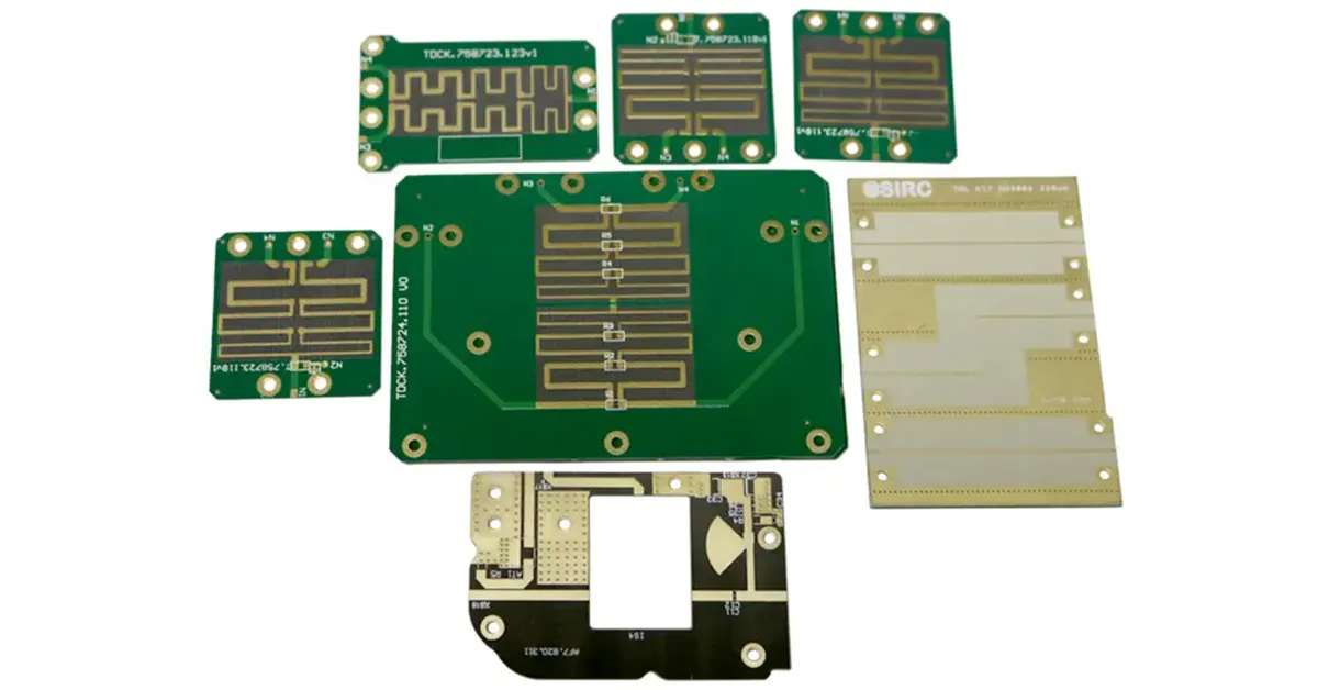
As wireless communication, radar, and high-speed digital systems continue to evolve, high-frequency PCB materials have become essential for reliable signal transmission. Selecting the right laminate, controlling impedance precisely, and designing a proper stack-up are the keys to a successful RF product.
From PTFE laminates and hydrocarbon resins to LCP and ceramic-filled composites, each family has its strengths — and every project balances electrical performance, manufacturing complexity, and cost. If you are weighing those trade-offs, our FR-4 vs Rogers materials comparison is a good next read.
Quick answers on materials, cost, and applications
A PCB is generally classified as a high-frequency PCB when it operates above 1 GHz. Applications involving microwave and millimeter-wave signals may operate at frequencies above 24 GHz or even 77 GHz.
Low dielectric loss reduces signal attenuation during transmission, helping maintain signal strength and improve communication reliability in high-speed and RF systems.
PTFE-based materials such as Rogers RO5880 and RO4350B are commonly used because they offer low loss, stable dielectric performance, and excellent high-frequency characteristics.
Yes. High-frequency PCB materials typically cost more due to specialized laminates, tighter manufacturing tolerances, and advanced impedance control requirements.
Major industries include telecommunications, automotive electronics, aerospace, satellite communication, defense systems, medical equipment, and high-speed networking.
Share your target frequency, material preference, and stack-up — we will confirm manufacturability and send a quote within one working day.
Get an RF PCB Quote Fast Reply on WhatsAppHigh-frequency PCBs are designed to support high-speed signal transmission with minimal loss, utilizing materials like Rogers to ensure low dielectric loss. Unlike standard PCBs, they prioritize signal integrity and thermal management.
As a pcb factory that has long specialized in advanced processes, high frequency pcb manufacturing has been our strength for many years, with significant market advantages in production quality management and cost control.
High-frequency PCB production refers to the manufacturing of printed circuit boards that operate at high frequencies, typically above 1GHz. These boards are designed to handle the specific requirements of high-frequency signals, ensuring low signal loss, minimal interference, and high signal integrity. They are used in applications such as wireless communications, radar systems, satellite communications, and high-frequency electronic devices.
Rapid Growth of Wireless Communication: Technologies like 5G and future wireless communication standards require high-frequency signals for faster data transfer and improved connectivity.
Internet of Things (IoT): The explosion in the number of IoT devices necessitates efficient and high-speed data transmission, which high-frequency PCBs provide.
Automotive Electronics: Advanced Driver Assistance Systems (ADAS) and autonomous driving technologies rely on high-frequency PCBs to process radar and sensor signals accurately.
Proliferation of High-Frequency Electronic Devices: Devices such as smartphones, tablets, and other high-frequency electronics require PCBs that can support higher data rates and better performance.
Here’s a detailed comparison table between High-Frequency PCBs and Standard PCBs, highlighting their key advantages, features, and technical distinctions:
| Aspect | High-Frequency PCBs | Standard PCBs | Detailed Explanation |
|---|---|---|---|
| Material Differences | Specialized Materials: PTFE, Rogers, ceramic substrates | FR4 Material: Commonly used, less effective at high frequencies | High-frequency PCBs use materials with low Dk and low Df, like Rogers RO4350B (Dk ~ 3.48, Df ~ 0.0037), which minimize signal loss and maintain signal integrity at high frequencies. Traditional PCBs use FR4, which has a higher Dk (~4.5) and Df (~0.02), leading to greater signal attenuation and distortion at higher frequencies. |
| Signal Integrity | Excellent: Maintains signal integrity, reduces reflection and interference | Lower: More susceptible to signal loss and interference | High-frequency PCBs are designed with strict impedance control and precise trace dimensions to maintain signal integrity even at GHz frequencies. For example, 50-ohm impedance control in high-frequency designs minimizes signal reflection. In contrast, standard PCBs may experience significant signal degradation at higher frequencies due to less stringent design requirements. |
| Thermal Management | Advanced: Effective heat dissipation through materials and design | Limited: Less effective, leading to heat buildup | High-frequency PCBs utilize materials with better thermal conductivity, like Rogers RO3003 (0.5 W/mK), and incorporate thermal vias and heat sinks to dissipate heat generated by high-frequency components. Standard PCBs, using FR4, have limited thermal management capabilities, often resulting in thermal hotspots and potential performance degradation. |
| Manufacturing Precision | High Precision: Strict control over impedance, trace widths, and spacing | Standard Precision: Suitable for general electronics | The manufacturing of high-frequency PCBs demands precise layer alignment, tighter tolerances (e.g., ±5% impedance tolerance), and accurate via drilling to ensure consistent performance across the board. For example, controlled impedance is crucial for minimizing signal loss in RF and microwave applications. Standard PCBs, on the other hand, have less stringent manufacturing requirements, adequate for low-frequency applications. |
| Application Range | High-Frequency Applications: Communication devices, radar, satellite, 5G | General Applications: Consumer electronics, computers, appliances | High-frequency PCBs are essential in high-frequency communication systems, radar systems, 5G base stations, and autonomous vehicle sensors, where signal integrity and thermal management are critical. For example, 5G base stations require PCBs that can handle mmWave frequencies. Standard PCBs are widely used in household electronics, computers, and consumer devices, where the operating frequency is lower, and the design requirements are less demanding. |
Here’s a detailed description of common high-frequency PCB materials and their specific models, focusing on Rogers and other popular brands:
Specializing in the production of high-frequency PCBs, we maintain a consistent stock of high-frequency materials. Please refer to our table of PCB substrate models with advanced manufacturing processes in the market. Due to the varying costs of different materials and the performance differences among brands and series, we offer competitive pricing on high-frequency substrates, with reliable and stable manufacturing processes.
Experience and Expertise: Choose a supplier with proven experience in high-frequency PCB production and a deep understanding of the specific requirements and challenges.
Material Availability: Ensure the supplier stocks a variety of high-frequency materials from reputable brands.
Manufacturing Capabilities: Verify that the supplier has the necessary equipment and processes to handle high-frequency PCB production, including precision drilling, lamination, and etching.
Quality Control: Look for suppliers with robust quality assurance protocols, including advanced testing and inspection capabilities.
Technical Support: Prefer suppliers who offer strong technical support and can assist with design optimization and troubleshooting.
References and Reviews: Check references and reviews from other clients to gauge the supplier’s reliability and performance.
Advanced Manufacturing Capabilities:
State-of-the-Art Equipment: Our facility is equipped with the latest high-precision manufacturing equipment capable of maintaining tight tolerances required for high-frequency PCB production.
Automated Processes: Utilization of automated production lines to ensure consistency, reduce human error, and increase efficiency.
Expertise and Skilled Workforce:
Experienced Engineers: Our team includes highly experienced engineers specialized in high-frequency PCB design and manufacturing, ensuring every aspect of the production process is optimized for performance and reliability.
Continuous Training: We invest in continuous training programs to keep our staff updated with the latest technologies and best practices in high-frequency PCB production.
Stringent Quality Control:
Comprehensive Testing: Implementing advanced testing protocols using sophisticated equipment like TDR (Time Domain Reflectometry) and VNA (Vector Network Analyzer) to verify signal integrity and performance.
Multi-Stage Inspection: Conducting thorough inspections at multiple stages of the production process, including Automated Optical Inspection (AOI), X-ray inspection, and final functional testing.
Superior Material Management:
High-Quality Materials: We use only the best high-frequency materials, such as Rogers, Taconic, and Isola, ensuring low dielectric constants and minimal signal loss.
Reliable Supply Chain: Maintaining strong relationships with material suppliers to ensure a steady supply of high-quality materials, avoiding delays and material inconsistencies.
Precision in Manufacturing:
Impedance Control: Precise control of impedance through careful manufacturing processes, ensuring signal integrity and reducing losses.
Thermal Management Solutions: Advanced thermal management designs to efficiently dissipate heat, preventing performance degradation in high-frequency applications.
Robust Process Control:
Tight Tolerance Manufacturing: Implementing processes that maintain tight tolerances on trace widths, spacings, and layer alignments to meet the exacting requirements of high-frequency PCBs.
Lean Manufacturing: Utilizing lean manufacturing principles to minimize waste and optimize production efficiency.
Strong Customer Support and Collaboration:
Design Assistance: Providing design support and consulting to help customers optimize their high-frequency PCB designs for manufacturability and performance.
Customized Solutions: Offering customized manufacturing solutions to meet specific customer needs and application requirements.
Continuous Improvement and Innovation:
R&D Investment: Investing in research and development to continuously improve our processes and stay at the forefront of high-frequency PCB technology.
Feedback Loop: Implementing a robust feedback loop with customers to learn from each project and continuously enhance our production capabilities.
We invite you to experience the excellence of our high-frequency PCB solutions. Whether you are in telecommunications, automotive, aerospace, or any other industry requiring high-frequency applications, our team is ready to deliver the quality and precision you need.