
PCB Via Guidelines for Multi-layer Circuit Board Manufacturing
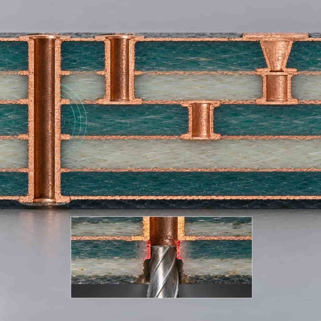
PCB Via Guidelines for Multi-layer Circuit Board Manufacturing Via families, parasitic behavior at RF, stub management with back-drilling, and the manufacturing rules — aspect ratio, filling, via-in-pad — that keep multilayer boards buildable. Table of Contents Vias look like the simplest feature on a multilayer board — a drilled hole, plated with copper — yet […]