High-Frequency PCB Insights & Resources

Technical guides, material comparisons and process insights on high-frequency, RF and microwave PCB manufacturing.

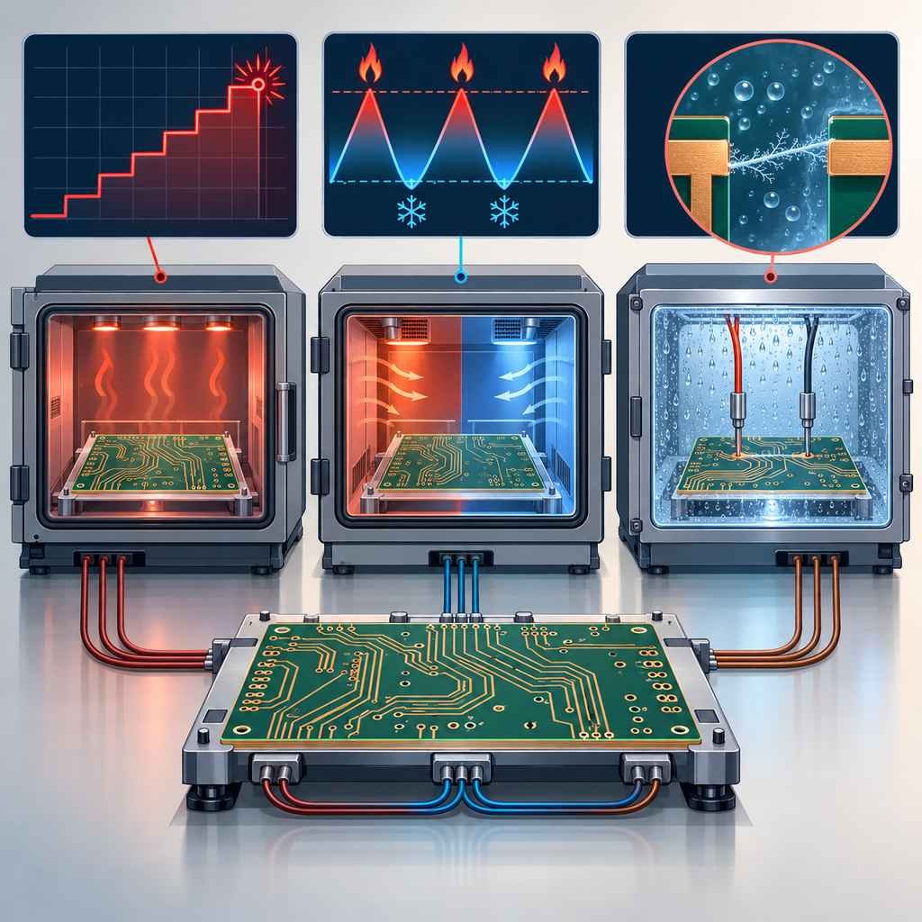
Three high-frequency PCB stress test stations for HALT step-stress, thermal shock cycles and CAF bias testing with a conductive filament inset

High-Frequency PCB Reliability Testing Guide: HALT Aging, Thermal Shock & CAF Test Procedures

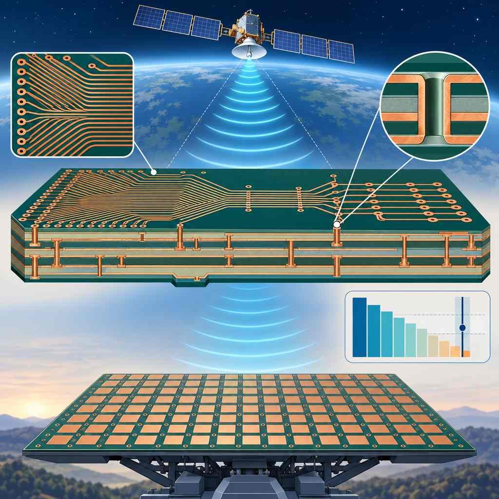
Satellite communication phased array antenna panel and its multilayer board with many mmWave channels, back-drilled vias and a loss budget bar

Satellite Communication Phased Array Antenna PCB Manufacturing: How to Achieve Low-Loss Transmission for 64-Channel Millimeter-Wave Signals?

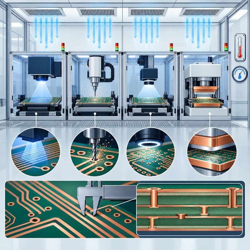
Cleanroom with four Rogers PCB process stations for imaging, drilling, AOI and ceramic pressing, holding a tight trace tolerance bracket

Revealing the Core Processes of Top Rogers PCB Manufacturers: How 5G Millimeter-Wave Boards Achieve ±0.02mm Tolerance

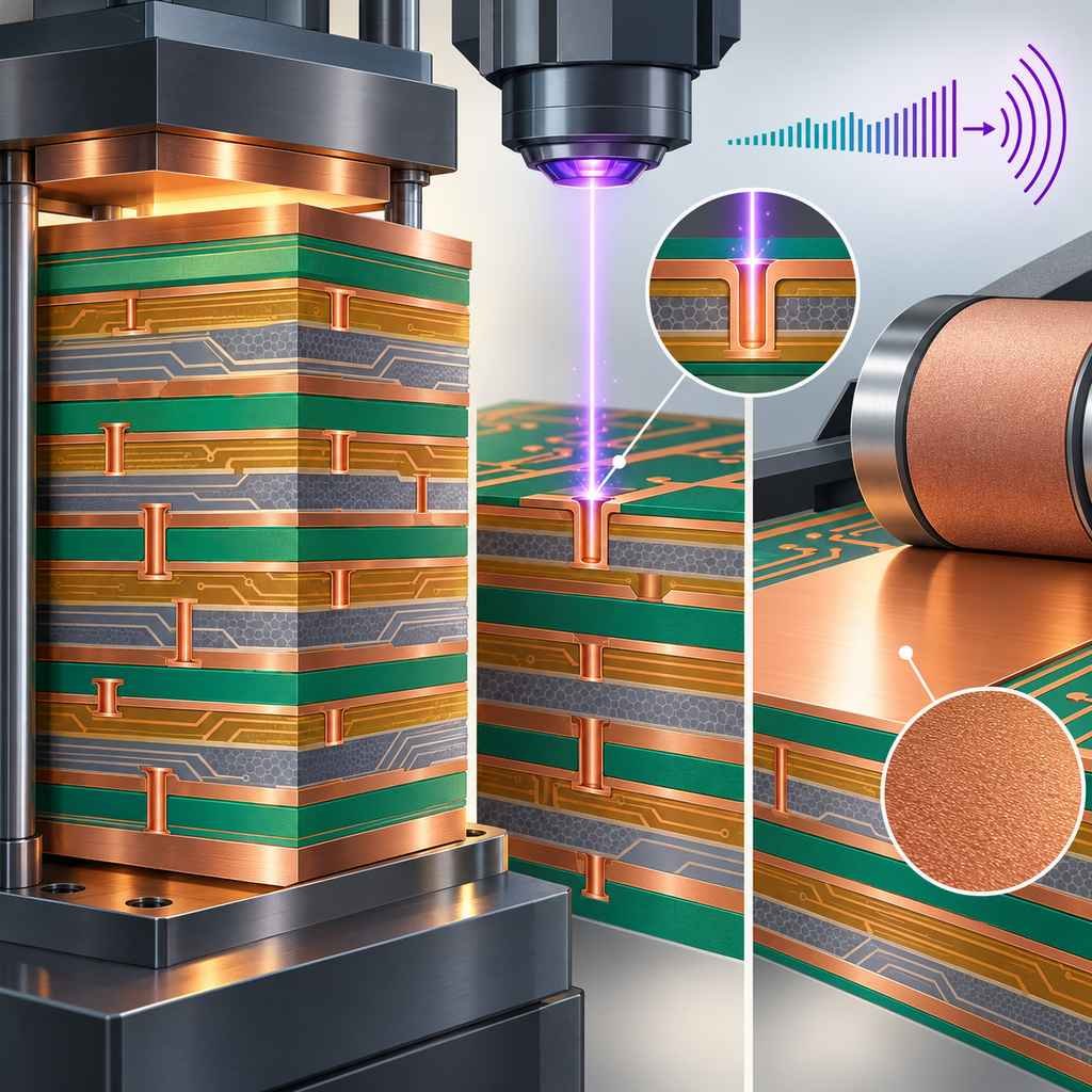
Hybrid PTFE multilayer stack under lamination beside UV laser microvia drilling and copper foil smoothing for 40 GHz and above boards

How Top Manufacturers Produce 40GHz+ High-Frequency PCBs: Deep Dive into PTFE Hybrid Lamination and Laser Drilling Technologies

Three certification seals for flammability, medical traceability and automotive quality attached to a high-frequency PCB

The 3 Must-Have Certifications for Rogers High-Frequency PCB Manufacturers: UL, ISO 13485, and IATF 16949 Explained

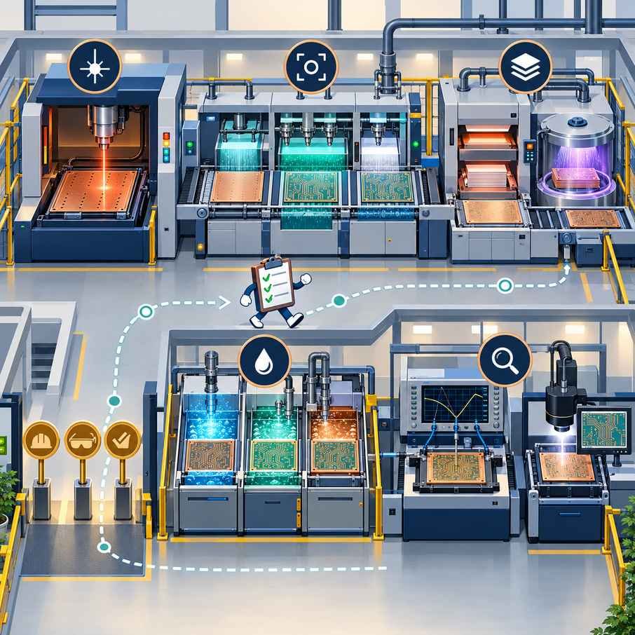
Factory floor audit path through laser drilling, imaging, lamination, surface finish and testing areas with an inspection clipboard

The Complete Guide to Auditing High-Frequency PCB Manufacturers: Essential Equipment from Laser Drilling to AOI Inspection

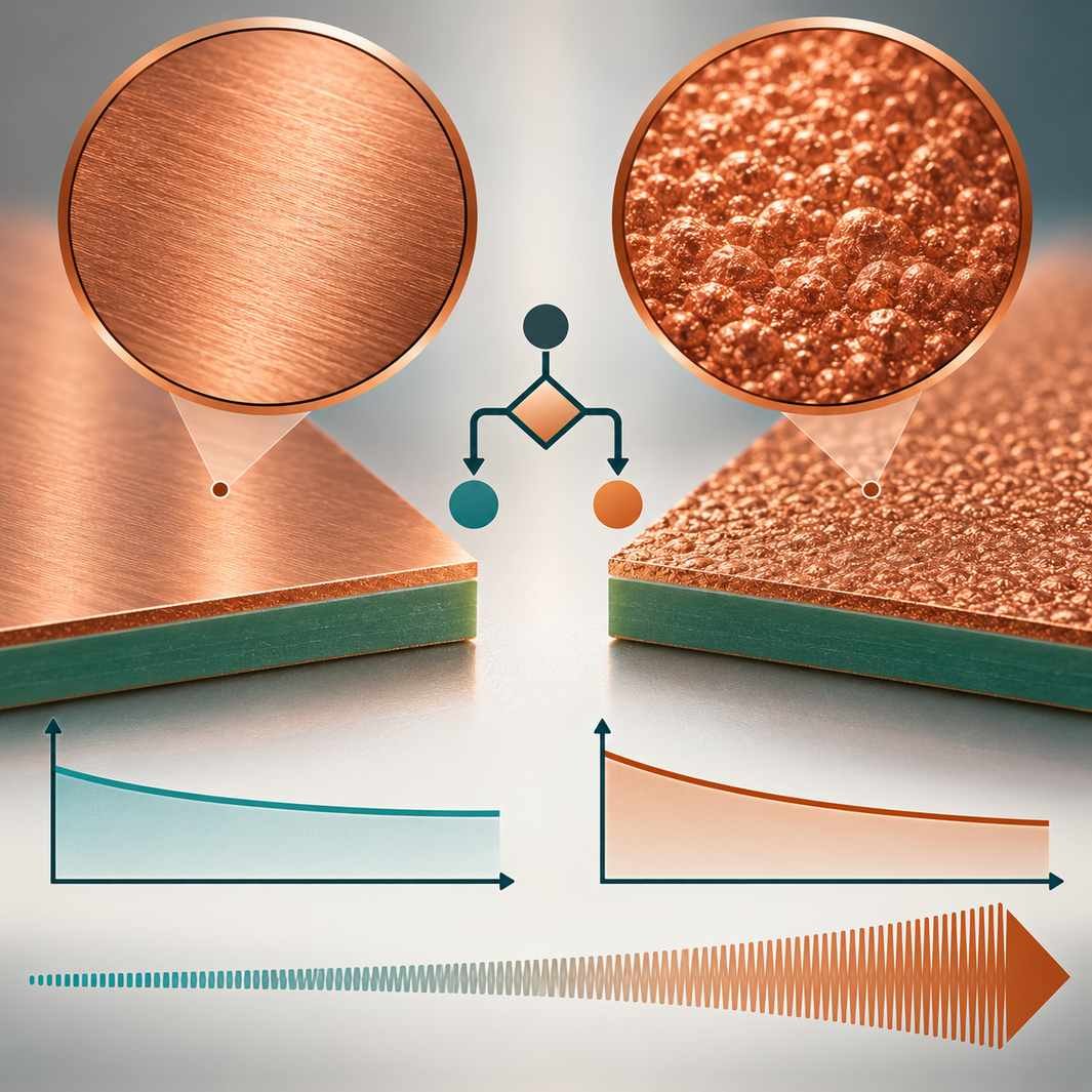
Low-roughness copper foil and reverse-treated foil surfaces magnified side by side above their loss curves and a frequency band strip

PCB Copper Surface Treatment for Millimeter-Wave Bands: Selection Guide Between Low-Roughness Copper vs. Reverse-Treated Foil

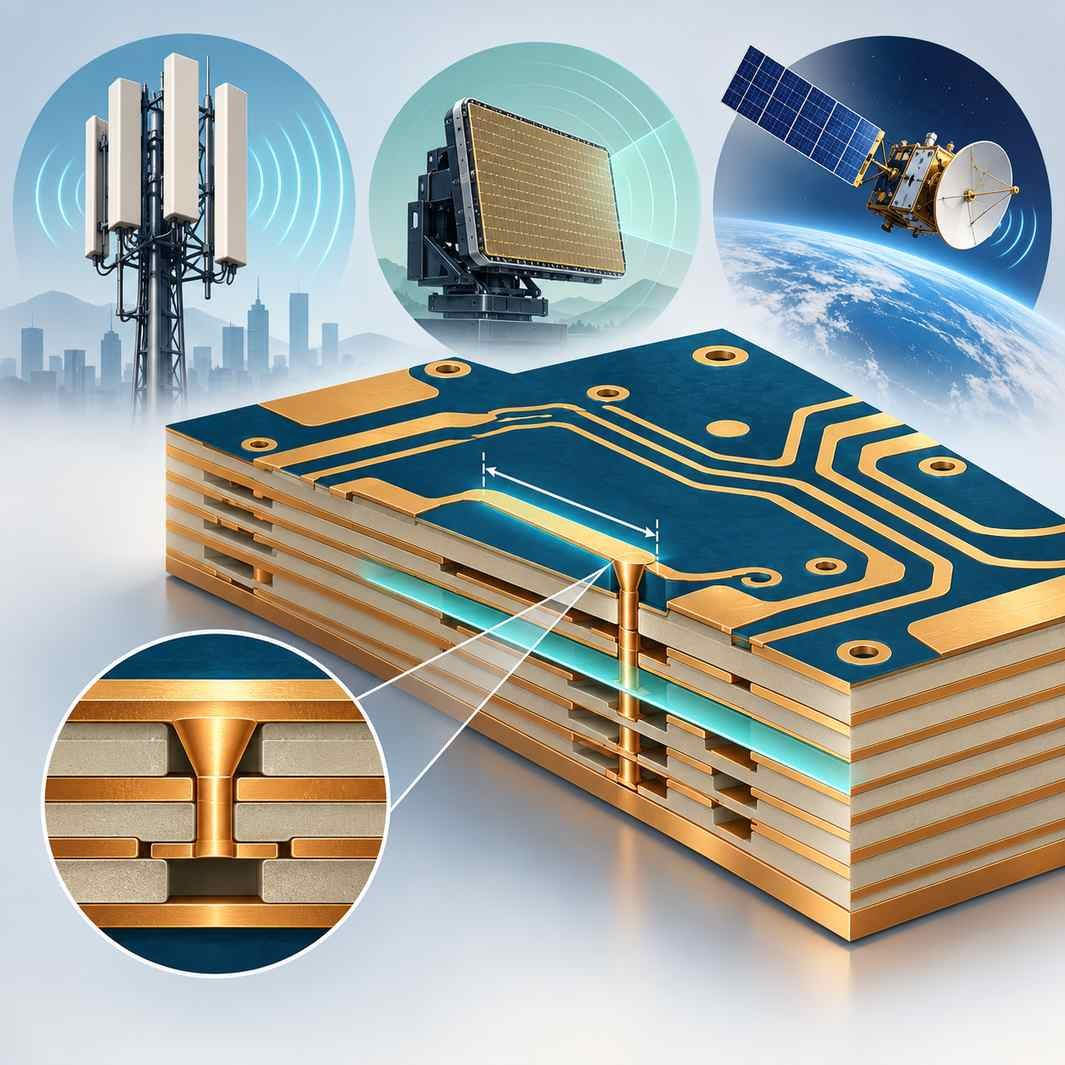
Ten-layer high-frequency board with laser microvias, an impedance tolerance bracket, shielding plane and 5G, radar and satellite applications

Characteristics of Multilayer High-Frequency PCBs: Technical Advantages and Application Value

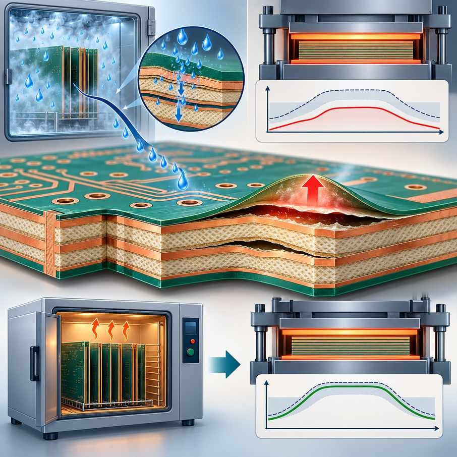
High-frequency PCB cross-section showing delamination and blistering from moisture absorption and low lamination temperature, with bake oven and press fixes

High-Frequency PCB Delamination & Blistering Deep Dive: Solving Moisture Absorption and Insufficient Lamination Temperature

RO4003C ceramic-filled laminate panel with dielectric, CTE and processability indicators and five application silhouettes

Analysis of Rogers 4003C Laminate Properties and Applications

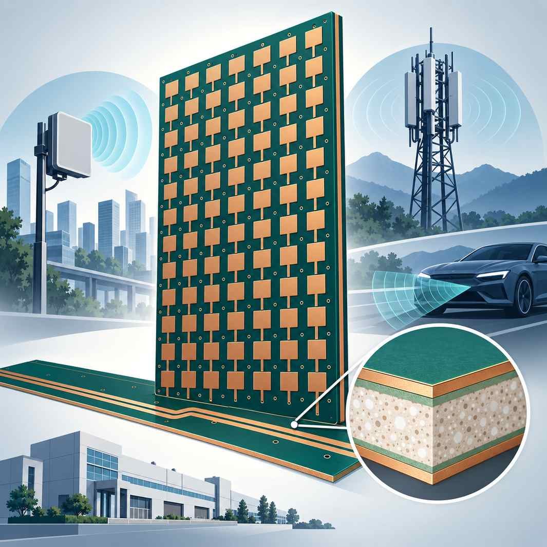
RO4350B massive MIMO array panel with millimetre-wave small cell, base station and automotive radar applications and a magnified laminate inset

High-Frequency PCB Material Selection Guide: Key Applications of Rogers RO4350B in 5G Communications

F4B and RO4350B laminate panels compared under a measuring bridge with cost tags, a decision ladder and magnified cores

Comprehensive Comparison: F4B vs. RO4350B High-Frequency Materials – Expert Analysis

PCB Assembly

PCBA Services

Quality

Application

Resources

Printed Circuit Board

RF PCB

Quality

PCB Surface Finish

Printed Circuit Board

Drills & Throughplating

Profiles

PCB Stackup

Resources