Rogers RO3000 PCB materials are ceramic-filled PTFE laminates developed for RF, microwave and high-frequency circuit applications. The series includes RO3003, RO3006, RO3010 and RO3035, offering different dielectric constants while maintaining broadly consistent mechanical characteristics across the material family.
For engineers developing radar systems, antennas, wireless communication equipment and multilayer RF circuits, selecting the right laminate involves more than comparing dielectric constant (Dk). Dissipation factor (Df), dimensional stability, copper foil type, laminate thickness and fabrication requirements must also be considered.
This guide reviews the key specifications and selection considerations for the Rogers RO3000 series, based on Rogers Corporation’s published material documentation.
Rogers RO3000 is a family of ceramic-filled PTFE circuit laminates designed for RF and microwave applications. The series includes RO3003, RO3006, RO3010 and RO3035, with process dielectric constants ranging from approximately 3.00 to 10.2. Each grade offers different electrical properties for specific circuit design requirements. Engineers should compare Dk, Df, laminate thickness, copper foil and fabrication compatibility before selecting a material.
The Rogers RO3000 series uses ceramic-filled PTFE composite technology to combine high-frequency electrical performance with dimensional stability. According to Rogers, the materials are designed to support commercial microwave and RF applications and multilayer constructions using different dielectric constants.
The main materials covered in this guide are:
RO3003: A low-Dk laminate intended for demanding RF and microwave circuits.
RO3006: A higher-Dk option for designs requiring greater dielectric loading and potential circuit-size reduction.
RO3010: A high-Dk laminate for applications where dielectric constant is an important design variable.
RO3035: A low-loss, ceramic-filled PTFE material offering a Dk of approximately 3.5.
These materials should not be treated as interchangeable. The appropriate grade depends on the operating frequency, electrical requirements, stack-up, transmission-line geometry and mechanical constraints of the design.
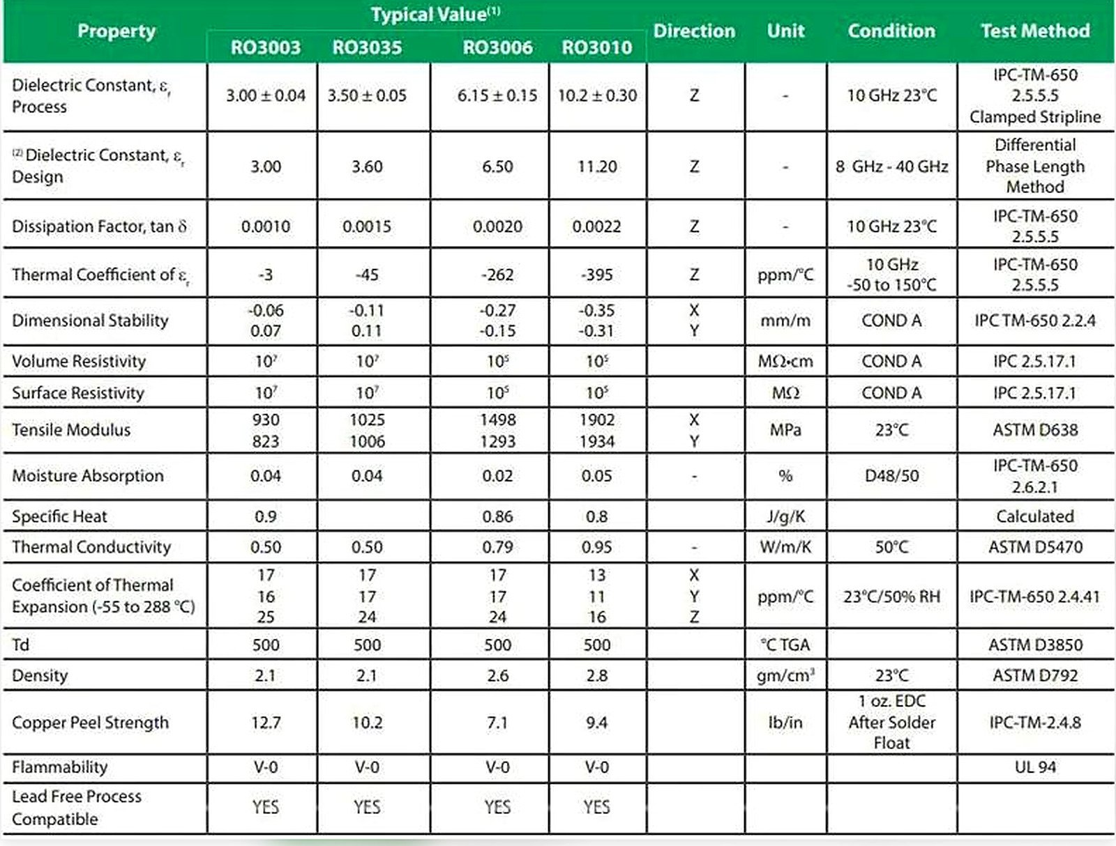
The following values are taken from the supplied Rogers RO3000 series datasheet. Process Dk and design Dk are shown separately because they serve different purposes in material characterization and circuit design.
| Parameter | RO3003 | RO3035 | RO3006 | RO3010 |
|---|---|---|---|---|
| Process Dk | 3.00 ± 0.04 | 3.50 ± 0.05 | 6.15 ± 0.15 | 10.2 ± 0.30 |
| Design Dk listed in supplied datasheet | 3.00 | 3.60 | 6.50 | 11.20 |
| Dissipation factor (Df) at 10 GHz, 23°C | 0.0010 | 0.0015 | 0.0020 | 0.0022 |
Source: supplied Rogers RO3000 series datasheet. Confirm the current manufacturer datasheet and applicable test conditions before using these values in a released design.
Dk affects the propagation of electromagnetic signals and the dimensions required for a target impedance. A higher Dk can help reduce circuit dimensions in some designs, but it also changes transmission-line geometry and electromagnetic behavior.
Df represents dielectric loss. Lower dielectric loss can be advantageous when designing circuits that must preserve signal strength at high frequencies.
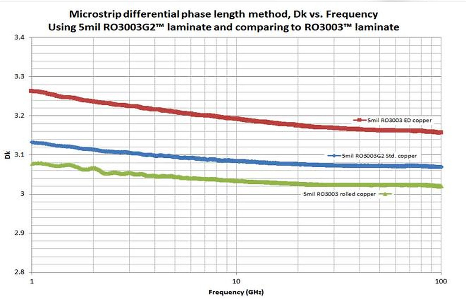
Material selection should therefore consider both parameters alongside copper roughness, dielectric thickness, conductor geometry and the intended operating frequency. A Dk value alone is not enough to predict insertion loss or overall RF performance.
The supplied datasheet lists the following standard thickness configurations.
| Material | Standard thicknesses |
|---|---|
| RO3003 | 0.13, 0.25, 0.51, 0.76 and 1.52 mm |
| RO3006 / RO3010 | 0.13, 0.25, 0.64 and 1.28 mm |
| RO3035 | 0.25, 0.51 and 1.52 mm |
The listed standard panel sizes include:
12 × 18 inches (305 × 457 mm)
18 × 24 inches (457 × 610 mm)
The supplied datasheet also lists a 24 × 21-inch (610 × 533 mm) panel option for certain RO3003 thicknesses.
These are documented standard configurations, not a guarantee that every grade and thickness is available for immediate shipment. Other dimensions and constructions should be confirmed with the material supplier.
Copper foil selection can influence conductor loss, etching performance and high-frequency signal integrity.
The supplied datasheet lists ½ oz (18 μm) and 1 oz (35 μm) copper options. RO3003 is listed with both electrodeposited copper foil and rolled copper foil, while the listed RO3006, RO3010 and RO3035 configurations specify electrodeposited copper.
For demanding RF applications, engineers should evaluate the copper foil profile and roughness in addition to nominal copper thickness. At higher frequencies, conductor surface characteristics can contribute to insertion loss.
The final copper selection should be based on current material availability, conductor geometry, power requirements and the electrical performance targets of the finished PCB.
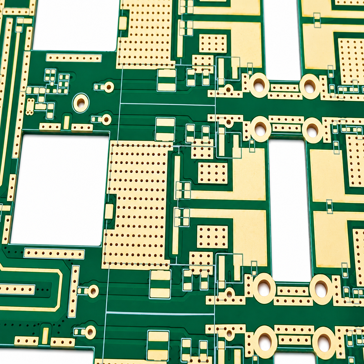
One advantage of the RO3000 family is its ability to support multilayer designs using materials with different dielectric constants. Rogers describes the series as having consistent mechanical properties across its Dk range, helping designers develop mixed-Dk constructions.
The supplied datasheet describes an in-plane thermal expansion coefficient of approximately 17 ppm/°C for the series and discusses the importance of matching expansion behavior to copper. The detailed product specifications should still be reviewed for the exact material grade and direction.
For hybrid PCB designs, engineers should confirm compatibility between the selected laminate, bonding materials and any other dielectric layers. Lamination temperature, pressure, resin flow, dimensional registration and plated-through-hole reliability must be considered during fabrication planning.
A successful hybrid stack-up requires both electrical design validation and a manufacturing process appropriate for the selected materials.
Rogers identifies several application areas for the RO3000 family, including:
Automotive radar and advanced driver-assistance systems (ADAS)
RF and microwave antennas
Cellular telecommunications equipment
Power amplifiers
Satellite communication systems
Wireless communication circuits
High-frequency multilayer PCB assemblies
The best material depends on the electrical and mechanical requirements of the individual application. For example, a low-Dk material may suit a compact RF transmission-line design, while a higher-Dk material may be considered when reducing circuit dimensions is a priority.
The selected material should always be validated against the intended frequency range, impedance requirements, thermal environment and complete stack-up.
Rogers states that RO3000 series laminates can be fabricated using standard PTFE circuit-board processing techniques with modifications described in its fabrication guidelines.
Before production, PCB engineers and manufacturers should confirm:
Exact laminate grade and nominal thickness.
Copper foil type, weight and surface characteristics.
Finished board dimensions and dimensional tolerances.
Required impedance values and tolerance.
Drilling, hole-wall preparation and copper-plating requirements.
Bonding materials and lamination conditions for multilayer constructions.
Electrical testing and inspection requirements.
PTFE-based materials may require process controls different from conventional FR-4 fabrication. The exact requirements depend on the laminate grade, stack-up and manufacturing method.
For this reason, a fabrication drawing, stack-up specification and Gerber data should be reviewed together before production is approved.
A practical selection process starts with the electrical design rather than choosing a laminate solely by its product name.
Choose RO3003 when a low-Dk material and low dielectric loss are important design considerations.
Evaluate RO3006 when a higher dielectric constant is required to support the intended circuit geometry.
Evaluate RO3010 for designs that call for a substantially higher dielectric constant and more compact circuit dimensions.
Consider RO3035 when its Dk, loss characteristics and mechanical requirements fit the target application.
These are initial selection guidelines, not substitutes for electromagnetic simulation or manufacturer data. Final selection should use the current datasheet, actual design Dk, copper properties, dielectric thickness and fabrication tolerances.
HF PCB Pro supports high-frequency PCB manufacturing inquiries involving material selection, stack-up review, controlled impedance and multilayer fabrication. Customers can provide their Gerber files, stack-up and technical specifications for engineering review and quotation.
RO3003 has a process Dk of 3.00 ± 0.04, while RO3006 has a process Dk of 6.15 ± 0.15 in the supplied datasheet. RO3006's higher dielectric constant can support smaller circuit dimensions in some designs, but the complete electrical layout must be evaluated.
The supplied datasheet lists a process Dk of 10.2 ± 0.30 and a design Dk of 11.20 for RO3010. Engineers should confirm the appropriate value and test conditions before completing impedance calculations.
Process Dk is a material characterization value. Design Dk is intended for circuit-design calculations under specified conditions. The values can differ, so engineers should use the appropriate manufacturer data for the intended application and design method.
Yes. Rogers describes the series as suitable for multilayer circuit constructions. Hybrid designs must account for bonding materials, lamination conditions, layer registration and compatibility between the selected dielectrics.
Not necessarily. The datasheet lists standard configurations, but actual stock depends on the material grade, thickness, copper cladding and supplier inventory. Confirm availability before finalizing the design.
Refer to the official Rogers RO3000 series product page, the manufacturer datasheet and the RO3000/RO3200 fabrication guidelines linked below. Always check the latest documentation before releasing production data.
For high-frequency PCB manufacturing support, visit the HF PCB Pro High-Frequency PCB page or contact our engineering team with your design files and material requirements.
Send us your stack-up and material combination. Our engineering team will review the lamination plan, drilling and plating strategy, then quote your hybrid RF board.
Get An Engineering Review → Fast Reply on WhatsApp