High-Frequency PCB Insights & Resources

Technical guides, material comparisons and process insights on high-frequency, RF and microwave PCB manufacturing.

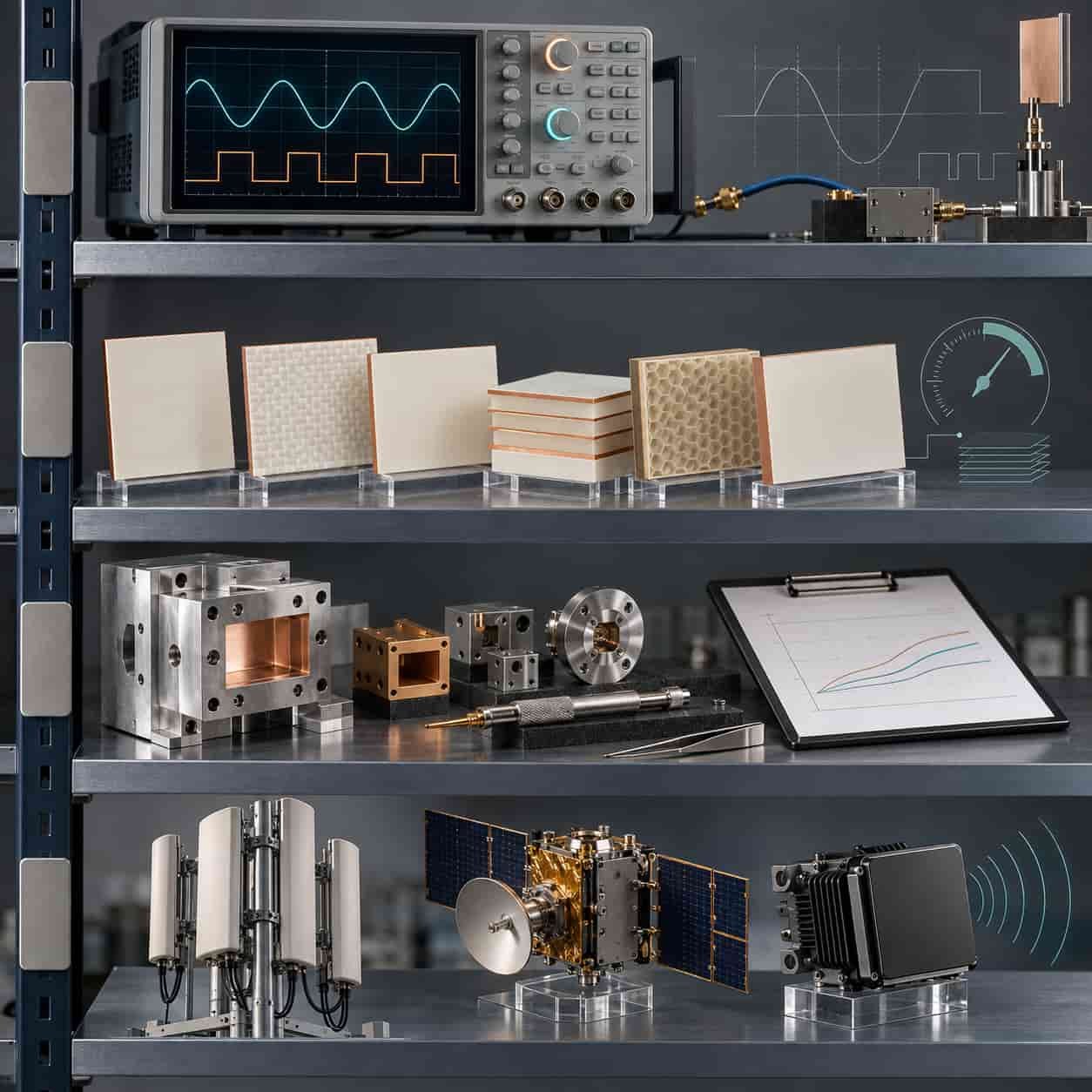
Four glossary layers for RF microwave PCB terms covering frequency and signal, material and impedance, manufacturing and test, and system level

RF and Microwave Terms in PCB design and manufacturing

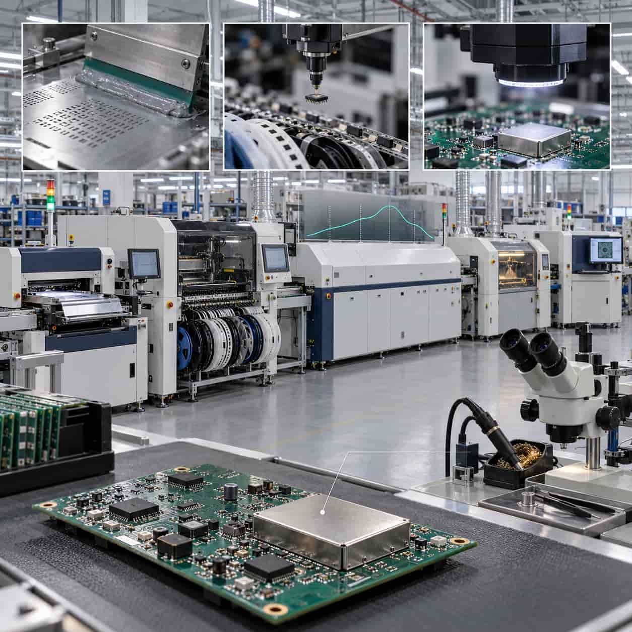
SMT assembly line from stencil printing and pick-and-place through reflow, wave soldering and AOI inspection, with a rework station and RF shield can

What is PCB Assembly Process ?

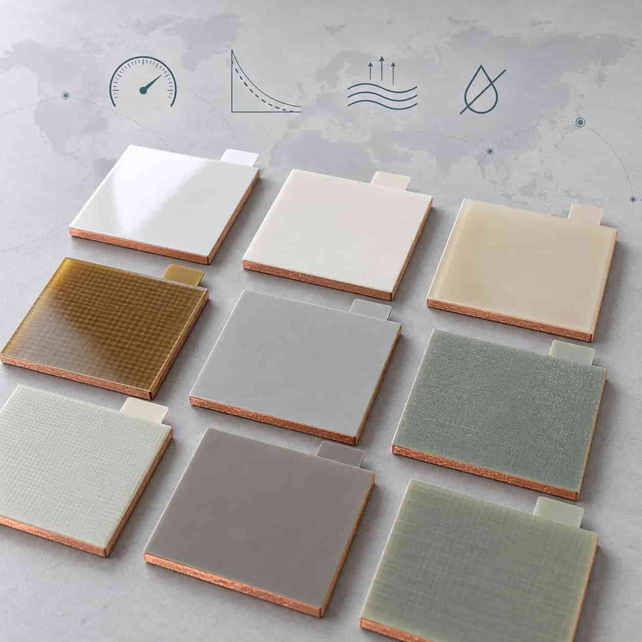
Grid of high-frequency laminate sample tiles with four specification icons above and a faded market map with factory markers behind

Basic Knowledge of HF PCB Materials, Manufacturers, and Specific Models

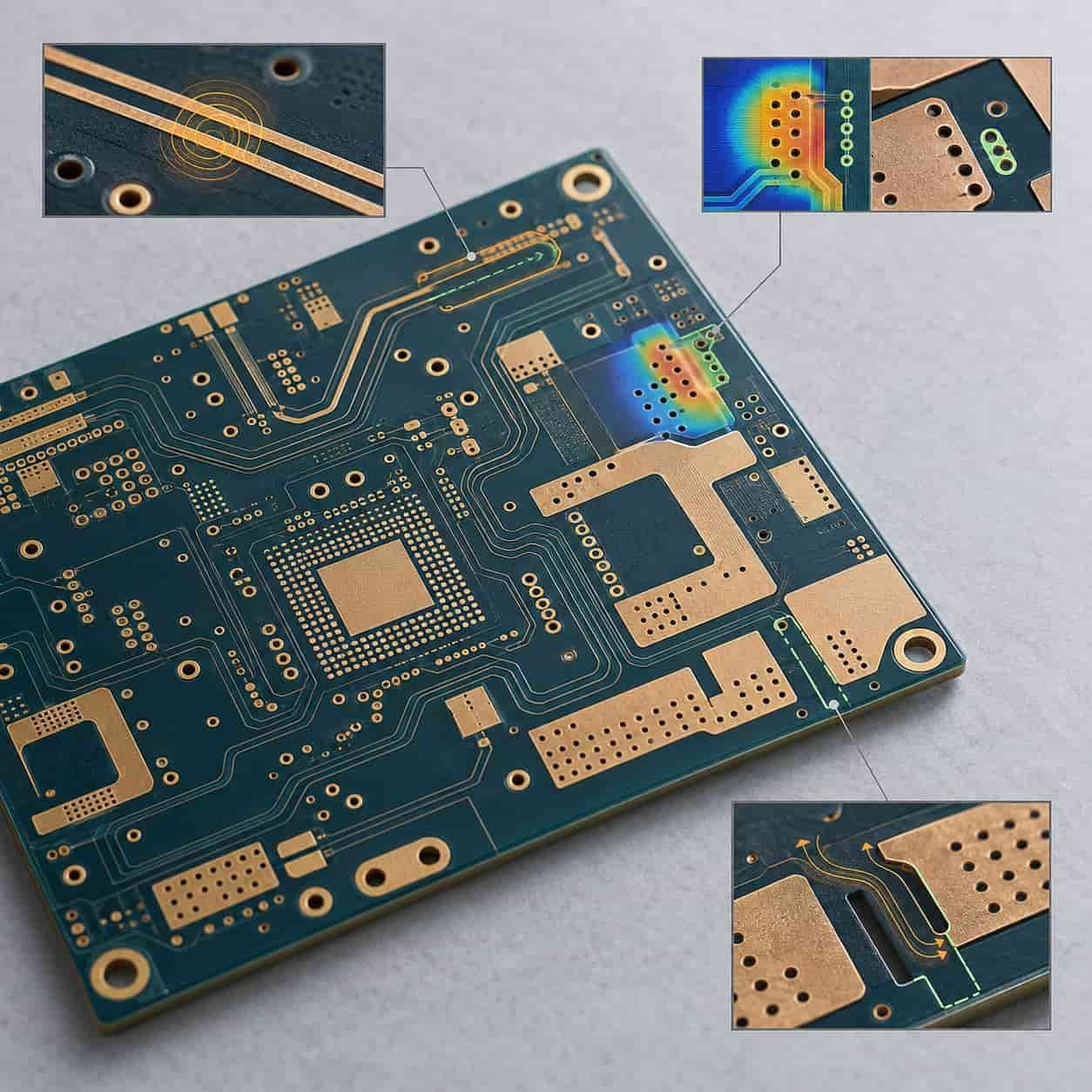
RF PCB layout with five highlighted design mistakes for impedance, return path, crosstalk, thermal and skipped simulation, each with a fix icon

Common Mistakes in RF PCB Design and How to Avoid Them

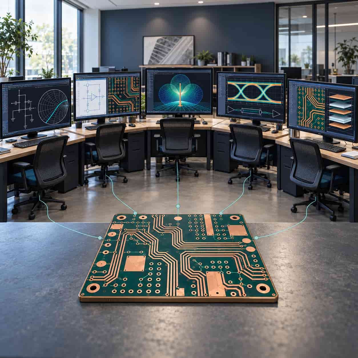
Five RF design workstations showing schematic, layout, 3D electromagnetic simulation, signal integrity and board editing around a shared high-frequency board

RF Microwave Circuit Board Design Tools

Sample excerpt-3
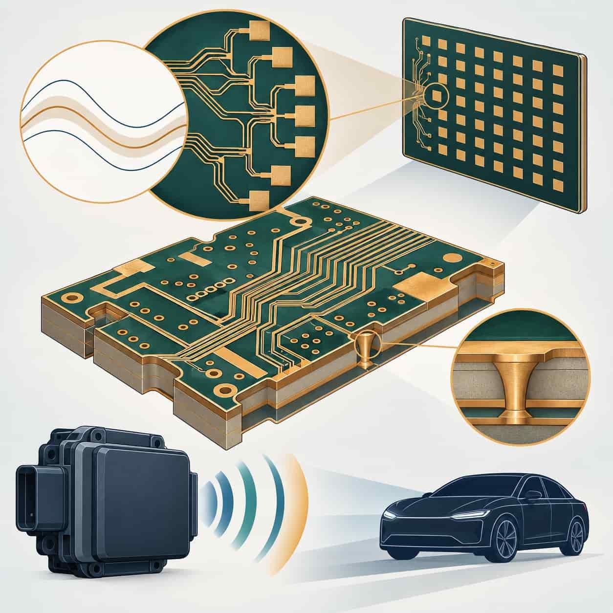
Millimeter-Wave-Radar-PCB-Materials-Design-Manufacturing

Millimeter-Wave Radar PCBs: Materials, Design, and Manufacturing Techniques

Sample excerpt-2
Three-axis tool selection diagram with 5G, automotive radar, aerospace and consumer medical application clusters linked to a design tool window

RF and Microwave Circuit Design: Tools and Application-Specific Recommendations

The process of PCB from design to production usually includes the following steps:

PCB Assembly

PCBA Services

Quality

Application

Resources

Printed Circuit Board

RF PCB

Quality

PCB Surface Finish

Printed Circuit Board

Drills & Throughplating

Profiles

PCB Stackup

Resources