A customer project called for a 12 layer high frequency PCB measuring approximately 150 mm × 150 mm, with a finished thickness of about 4 mm. The customer specified a domestically sourced laminate with a nominal dielectric constant of 3.38, together with backdrilling and plated over filled via technology, commonly known as POFV.
The manufacturing focus was the interaction between the multilayer stackup and the different hole structures. Material selection established the starting point, while stackup review, drilling requirements and via filling requirements determined how the design could be translated into a practical fabrication plan.
| Parameter | Customer Requirement |
|---|---|
| Board dimensions | Approximately 150 mm × 150 mm |
| Copper layers | 12 |
| Finished board thickness | Approximately 4 mm |
| Base material | Domestically sourced high frequency laminate |
| Specified dielectric constant | Nominal Dk 3.38 |
| Special drilling requirement | Backdrilling |
| Via filling requirement | POFV |
The Dk value represents the customer’s material requirement. The exact laminate grade, test frequency, test method and tolerance still need to be identified in the approved material specification. Dissipation factor and thermal properties also require review before material substitution or production approval.
A 12 layer board with a finished thickness of approximately 4 mm requires careful coordination of dielectric thicknesses, copper weights and lamination behavior.
Where controlled impedance is required, the distance between a trace and its reference plane affects the necessary trace geometry. Stackup approval therefore needs to address the electrical structure as well as the overall mechanical thickness.
The bonding system also matters. A core laminate with a nominal Dk of 3.38 does not establish the dielectric properties of every insulating layer in the finished board. Bonding materials and their thickness after lamination must be included in the engineering review.
![Approved 12 Layer Stackup Drawing] Suggested caption: Stackup for the customer’s 12 layer high frequency PCB, showing the approved materials, dielectric thicknesses and copper layers.](https://hfpcbpro.com/wp-content/uploads/Lamination-Diagram-for-a-12-Layer-High-Frequency-PCB.png "12 Layer High Frequency PCB Case Study Using Domestic Dk 3.38 Material with Backdrilling and POFV 1")
A plated hole can extend beyond the layers needed for an electrical connection. The unused section of the plated barrel forms a stub that may affect signal transmission.
Backdrilling uses a controlled depth drilling operation to remove the unwanted copper barrel over a specified portion of the hole. Its purpose is to reduce the electrical influence of that unused section.
For this approximately 4 mm thick board, the backdrill definition needs to establish the entry side, retained connection layer, backdrill diameter, allowable residual stub and depth tolerance. Clearance to nearby copper must also be checked.
Drilling deeper does not automatically produce a better result. Insufficient depth can leave an excessive stub, while excessive depth can damage a connection that must remain intact. Clear layer references and tolerances are essential.
POFV stands for Plated Over Filled Via. The hole is filled and planarized before a plated metal cap is formed over its surface. This construction is commonly used where a pad must extend over a via or where surface flatness is important.
For this project, the fabrication requirements need to identify which holes require POFV, the filling material and the cap requirements. The term POFV alone does not specify whether the fill must be conductive.
Process review should address filling completeness, curing, planarization and the continuity of the plated cap. Where the resulting pad supports component assembly, acceptable surface depression or protrusion should be defined in the customer’s acceptance requirements.
Backdrilling and POFV serve different purposes, so their presence on the same board requires a coordinated hole review.
The engineering data should distinguish standard plated holes, filled and capped vias, and holes requiring backdrilling. Any overlap between these groups needs to be identified before the manufacturing sequence is established.
The appropriate sequence depends on the actual hole structure and its relationship to lamination, plating, filling and subsequent drilling. A single standard sequence should not be assumed for every design.
For this project, a clearly marked hole table is particularly useful because the thick multilayer construction combines several hole processing requirements.
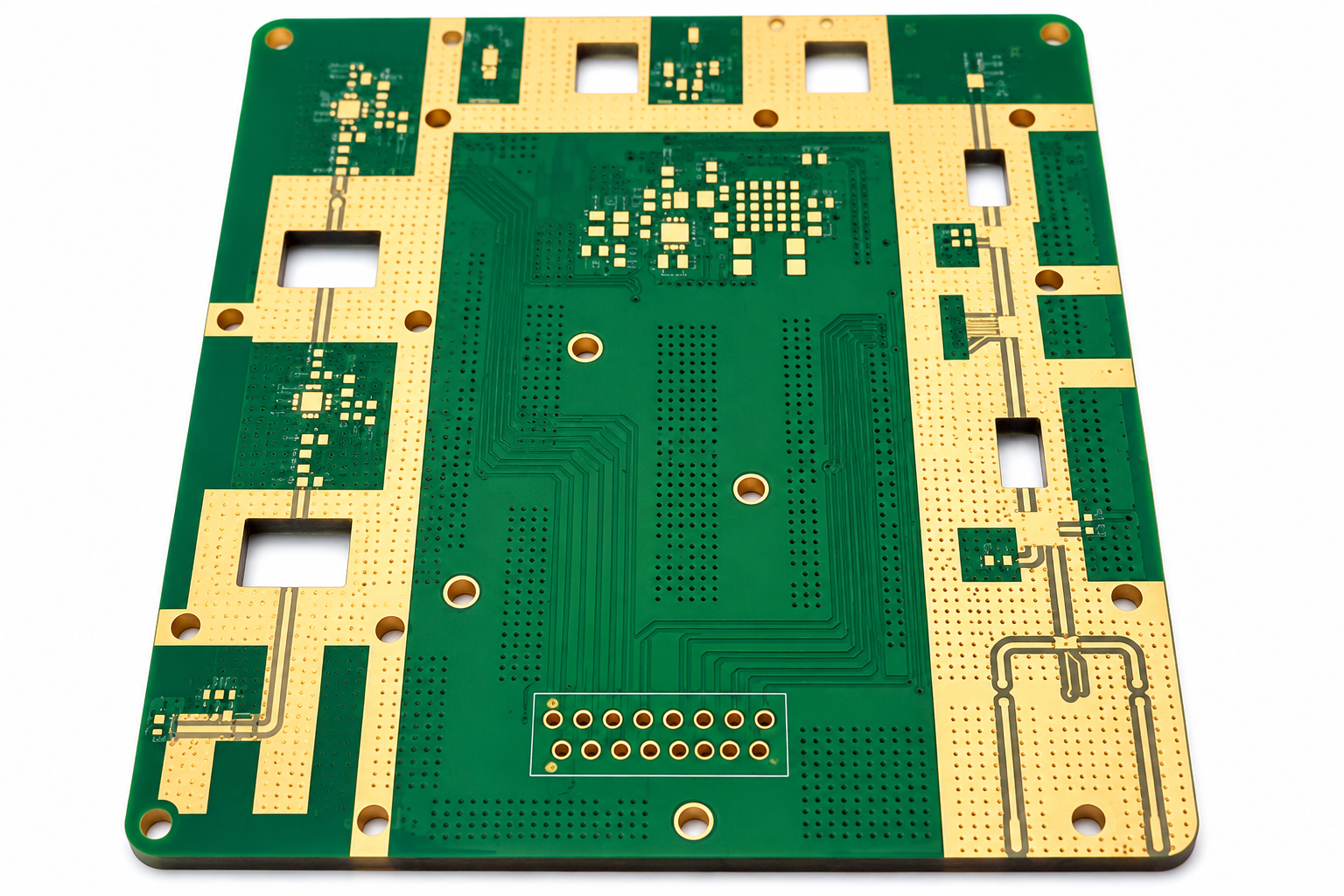
The board thickness also affects drilling and hole metallization. Smaller, deeper holes generally place greater demands on drilling quality, hole wall preparation and copper distribution within the barrel.
The minimum finished hole diameter has not been specified in the available project information, so a project aspect ratio cannot be stated. Likewise, the required hole wall treatment must be selected according to the actual laminate chemistry. A nominal Dk of 3.38 alone does not establish whether a PTFE specific process is appropriate.
Inspection planning should follow the customer’s acceptance criteria. Relevant checks may include finished thickness, layer registration, hole copper, via filling, cap quality and backdrill depth or residual stub. Any required impedance or RF performance testing needs its own agreed test structures and acceptance limits.
This customer project combines domestic Dk 3.38 material, 12 copper layers, an approximately 4 mm finished thickness, backdrilling and POFV in one PCB.
The case highlights the need to review materials, stackup and hole processing together. Each requirement affects the fabrication plan, and the interfaces between them deserve as much attention as the individual processes.
For similar projects, Gerber or ODB++ data, stackup requirements, a hole table, backdrill layer definitions and clearly identified POFV locations support a more accurate manufacturability review and quotation.
A matching Dk is insufficient to establish equivalence. Dissipation factor, measurement conditions, thickness tolerances, thermal expansion, copper foil and bonding materials also need comparison. Electrical validation may be necessary.
No. The need depends on connection layers, unused via length, operating frequency or signal edge rate, and the design's allowable loss and reflection.
No. POFV describes a filled via with a plated cap. Whether the filling material must be conductive should be specified separately.
Send us your stack-up and material combination. Our engineering team will review the lamination plan, drilling and plating strategy, then quote your hybrid RF board.
Get An Engineering Review → Fast Reply on WhatsApp