
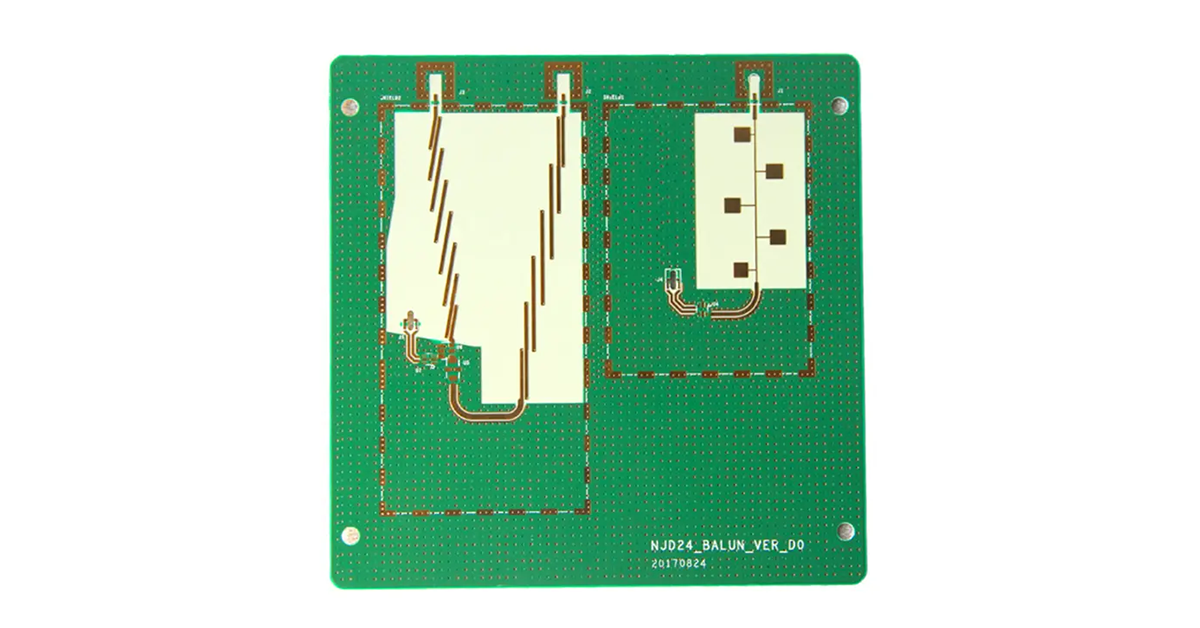
High-Speed High-Frequency PCB Design Guide | Controlled Impedance & RF PCB Layout Techniques
Learn advanced high-speed high-frequency PCB design techniques including controlled impedance, low-loss RF materials, stripline routing, back drilling, EMI suppression, and signal integrity optimization for reliable GHz-level performance.
high-speed-high-frequency-pcb-design-guide
High-Speed High-Frequency PCB Design Guide
High-speed high-frequency PCB design has become essential in modern industries such as 5G communications, radar systems, aerospace electronics, automotive ADAS, satellite devices, and AI data centers. As operating frequencies move into multi-GHz ranges, traditional PCB design methods are no longer sufficient. Engineers must now focus on signal integrity, impedance control, electromagnetic compatibility, and transmission loss management.
Unlike standard digital boards, RF and high-speed PCBs behave more like controlled electromagnetic structures than simple electrical connections. Every trace, via, dielectric layer, and reference plane directly affects signal quality.
This guide explains the key principles behind reliable high-speed high-frequency PCB design and how advanced PCB technologies help maintain stable signal transmission under extreme operating conditions.
1. Low-Loss PCB Materials Are the Foundation
Traditional FR-4 materials suffer from relatively high dielectric loss (Df) at high frequencies. As signal frequencies increase, FR-4 converts more electrical energy into heat, causing signal attenuation, timing instability, and poor insertion loss performance.
For this reason, high-frequency PCB manufacturers commonly use advanced RF laminate materials from companies such as:
- Rogers Corporation
- Taconic Advanced Dielectric Division
- Panasonic Megtron Materials
These materials provide:
- Low dielectric loss tangent (Df 0.0005–0.002)
- Stable dielectric constant (Dk 2.2–3.5)
- Reduced insertion loss
- Better phase consistency
- Improved impedance stability
Low-loss laminates are critical for maintaining signal fidelity in RF PCB design, microwave circuits, and high-speed digital interfaces above 10Gbps.
Comparison chart of FR-4 vs Rogers material loss performance at different frequencies


2. Controlled Impedance Is No Longer Optional
In high-speed PCB layout, impedance is not simply a target value. It must remain within strict tolerances.
Common controlled impedance structures include:
- 50Ω single-ended traces
- 100Ω differential pairs
- 85Ω USB differential routing
- 90Ω LVDS interfaces
Modern RF PCB fabrication typically controls impedance within ±5% or tighter.
Accurate impedance matching minimizes signal reflection and ensures maximum power transfer between the transmitter and receiver. Engineers achieve this by carefully controlling:
- Trace width
- Copper thickness
- Dielectric thickness
- PCB stack-up
- Material Dk values
Without proper impedance control, high-frequency signals experience reflections, eye diagram degradation, jitter, and data errors.
3. Microstrip and Stripline Routing
Transmission line structure selection is one of the most important aspects of high-speed PCB design.
Microstrip Routing
Microstrip traces are located on the outer PCB layer and reference a nearby ground plane.
Advantages:
- Lower propagation delay
- Easier tuning and debugging
- Lower manufacturing complexity
Disadvantages:
- Higher EMI radiation
- Greater susceptibility to external interference
Stripline Routing
Stripline traces are embedded between reference planes inside the PCB.
Advantages:
- Excellent shielding performance
- Extremely low radiation
- Better noise immunity
Disadvantages:
- Higher insertion loss
- More difficult fabrication
- Larger signal delay
Most advanced multilayer PCB designs use a combination of microstrip and stripline routing depending on signal sensitivity and routing distance.
Microstrip vs stripline PCB cross-section illustration


4. Routing Optimization and Differential Pair Matching
At GHz frequencies, even small routing discontinuities can create severe signal problems.
Rounded Corners Instead of Sharp Angles
High-frequency traces should avoid 90-degree corners. Engineers typically use curved or arc routing to reduce impedance discontinuities and minimize harmonic radiation.
Differential Pair Length Matching
Differential pairs require extremely tight length matching between P and N traces. Typical tolerances are:
- ≤0.5 mm
- or ≤5 mil
Proper length matching ensures synchronized signal arrival times and reduces common-mode noise.
Dense “accordion” style serpentine routing should be avoided because it increases unwanted coupling and impedance variation.
5. Via Optimization and Back Drilling
Vias introduce parasitic capacitance and inductance that become increasingly problematic at high frequencies.
Back Drilling Technology
Back drilling removes unused via stubs after layer transitions.
Benefits include:
- Reduced signal resonance
- Lower reflection
- Improved insertion loss
- Wider usable bandwidth
Back drilling is considered essential for 10Gbps, 25Gbps, and higher-speed PCB applications.
Smaller Via Structures
Modern high-density RF PCB manufacturing often uses:
- 0.2 mm mechanical vias
- Laser microvias
- HDI structures
Smaller vias reduce parasitic effects and improve signal transition quality.
PCB via stub and back drilling comparison


6. Ground Plane Integrity and Return Paths
Every high-speed signal requires a clean return current path.
A continuous reference plane beneath signal traces helps:
- Minimize loop inductance
- Reduce EMI radiation
- Lower ground bounce noise
- Improve signal stability
High-speed clock lines and RF signals should never cross split planes or gaps in the reference layer because this forces return current detours and creates electromagnetic interference problems.
Ground via stitching is also widely used to create low-inductance return paths and improve shielding effectiveness.
7. Solder Mask and Surface Finish Selection
In many RF PCB applications, solder mask is removed from critical RF traces.
The reason is simple: conventional solder mask materials often have unstable dielectric properties and higher loss at microwave frequencies.
Common high-frequency surface finishes include:
- ENIG (Electroless Nickel Immersion Gold)
- Immersion Silver
- OSP
Because of skin effect, high-frequency current flows only along the outer surface of the conductor. Smooth surface finishes significantly reduce conductor loss.
8. EMI and Crosstalk Suppression
As signal density increases, crosstalk and EMI become major challenges.
3W Spacing Rule
Adjacent traces should maintain spacing at least three times the trace width to reduce electromagnetic coupling.
Shielding and Via Fencing
Additional EMI suppression methods include:
- Ground copper along PCB edges
- Via fencing
- RF shielding covers
- Microwave absorbing materials
These techniques help contain electromagnetic radiation and improve overall EMC performance.
Conclusion
High-speed high-frequency PCB design is fundamentally about controlling electromagnetic wave behavior inside PCB structures. Every design decision — from low-loss RF materials and controlled impedance to back drilling and return-path optimization — directly impacts signal quality and system reliability.
As data rates continue to increase and communication systems move deeper into microwave frequencies, advanced PCB layout techniques are no longer optional. They are essential for achieving stable, low-loss, high-performance electronic systems.