
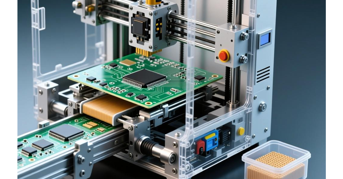
Learn the differences between FR-4 and RO4250B PCB materials, their lamination processing requirements, drilling considerations, reliability testing, and best practices for manufacturing high-frequency PCBs with superior performance and stability.
/fr4-ro4250b-pcb-lamination-processing-guide
FR-4 and RO4250B PCB Lamination Processing Guide
FR-4 and RO4250B PCB lamination processing plays a critical role in determining the performance, reliability, and manufacturability of modern electronic products. As high-frequency communication systems, automotive radar, satellite communications, and RF devices continue to evolve, engineers increasingly combine traditional FR-4 materials with high-frequency laminates such as RO4250B to balance performance and cost.
Understanding the material characteristics and processing requirements of both substrates is essential for achieving stable impedance control, reliable interconnections, and long-term product reliability.
Understanding FR-4 PCB Material
FR-4 remains the most widely used PCB substrate material in the electronics industry due to its excellent balance of performance and affordability.
Key Characteristics of FR-4
- Excellent mechanical strength
- Good electrical insulation properties
- Reliable thermal stability
- Strong chemical resistance
- Mature and cost-effective manufacturing process
- Suitable for multilayer PCB fabrication
The dielectric constant and loss tangent of FR-4 are acceptable for many digital and low-frequency applications. However, as operating frequencies increase, signal losses become more significant, making alternative materials necessary for RF and microwave circuits.
Typical Applications of FR-4
- Consumer electronics
- Industrial control systems
- Power supplies
- Computer motherboards
- Automotive electronics
Understanding RO4250B High-Frequency PCB Material
RO4250B is a high-performance laminate designed specifically for RF and microwave applications. Compared with FR-4, it offers significantly improved electrical characteristics at high frequencies.
Key Characteristics of RO4250B
- Low dielectric constant (Dk)
- Low dissipation factor (Df)
- Excellent dimensional stability
- High glass transition temperature (Tg)
- Consistent impedance performance
- Superior high-frequency signal transmission
These characteristics make RO4250B an ideal choice for designs operating in GHz frequency ranges where signal integrity is critical.
Typical Applications of RO4250B
- 5G communication equipment
- RF front-end modules
- Satellite communication systems
- Microwave circuits
- Automotive radar
- Wireless infrastructure equipment
For detailed material specifications, engineers can reference:
- https://rogerscorp.com/advanced-electronics-solutions
- https://www.ipc.org
- https://www.microwavejournal.com
Key PCB Lamination Processes for FR-4 and RO4250B
Although FR-4 and RO4250B have different electrical characteristics, their PCB manufacturing processes share many similarities.
Lamination Process
The lamination stage bonds multiple layers together under carefully controlled temperature and pressure conditions.
Critical parameters include:
- Lamination temperature profile
- Pressure control
- Vacuum environment
- Resin flow management
- Cure cycle duration
For hybrid stack-ups containing both FR-4 and RO4250B materials, special attention must be paid to differences in thermal expansion coefficients to prevent warpage and delamination.
PCB lamination press used for multilayer high-frequency PCB manufacturing.
Pre-Lamination Preparation
Proper preparation significantly improves production yield and reliability.
Material Inspection
Before lamination, all materials should be inspected for:
- Surface contamination
- Scratches
- Cracks
- Moisture absorption
- Dimensional defects
Layer Alignment
Accurate registration is critical for multilayer PCB fabrication.
Misalignment can result in:
- Impedance variation
- Via breakout
- Signal integrity issues
- Assembly defects
Prepreg Selection
For FR-4 laminates, prepreg quality directly impacts:
- Resin flow
- Bonding strength
- Dielectric consistency
- Final board thickness
Drilling Considerations
Drilling is one of the most critical processes in FR-4 and RO4250B PCB manufacturing.
Drill Bit Selection
Appropriate drill bit materials and geometries should be selected to reduce:
- Burr formation
- Glass fiber pull-out
- Hole wall roughness
- Thermal damage
Process Optimization
Key drilling parameters include:
- Spindle speed
- Feed rate
- Entry material
- Backup material
Optimized drilling improves plated-through-hole reliability and overall product quality.

High-precision CNC drilling process for high-frequency PCB fabrication.
Hole Wall Metallization
After drilling, copper plating creates electrical connections between PCB layers.
Electrolytic Copper Plating
A high-quality plated copper layer should provide:
- Uniform thickness
- Strong adhesion
- Low electrical resistance
- Excellent thermal cycling performance
Poor plating quality can lead to barrel cracking and intermittent electrical failures during product operation.
Laminate Stack-Up Design
The stack-up design directly affects impedance control and signal performance.
Design Considerations
Engineers should optimize:
- Core thickness
- Dielectric spacing
- Copper weight
- Reference plane placement
- Controlled impedance structures
When combining FR-4 and RO4250B, simulation tools should be used to verify impedance consistency across different material interfaces.
Reliability Testing
Reliability testing validates PCB performance under real-world operating conditions.
Thermal Cycling Test
Thermal cycling evaluates:
- Via reliability
- Layer adhesion
- Material stability
Damp Heat Test
Humidity testing evaluates:
- Moisture resistance
- Electrical insulation performance
- Long-term durability
These tests are especially important for telecommunications and aerospace applications.
Process Optimization and Quality Control
Production Automation
Modern automated production lines help improve:
- Manufacturing consistency
- Yield rates
- Production efficiency
AOI Inspection
Automated Optical Inspection (AOI) identifies:
- Open circuits
- Short circuits
- Etching defects
- Surface contamination
X-Ray Inspection
For hidden structures such as BGAs and buried vias, X-ray inspection verifies solder joint and internal connection quality.
Environmental and Safety Considerations
Manufacturers should implement proper ESD protection throughout production to prevent electrostatic damage.
For environmentally conscious designs, halogen-free FR-4 materials are increasingly being adopted to meet global environmental regulations and sustainability requirements.
Conclusion
Successful FR-4 and RO4250B PCB lamination processing requires a comprehensive understanding of material properties, manufacturing parameters, and quality control procedures. While FR-4 remains the preferred choice for general electronics, RO4250B offers superior performance for high-frequency PCB applications where signal integrity and low loss are critical.
By optimizing lamination, drilling, copper plating, stack-up design, and reliability testing, manufacturers can achieve highly reliable hybrid PCB structures that meet the demanding requirements of modern RF, microwave, and 5G communication systems.