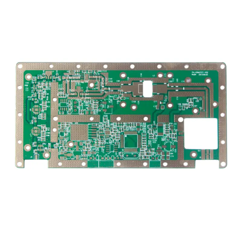
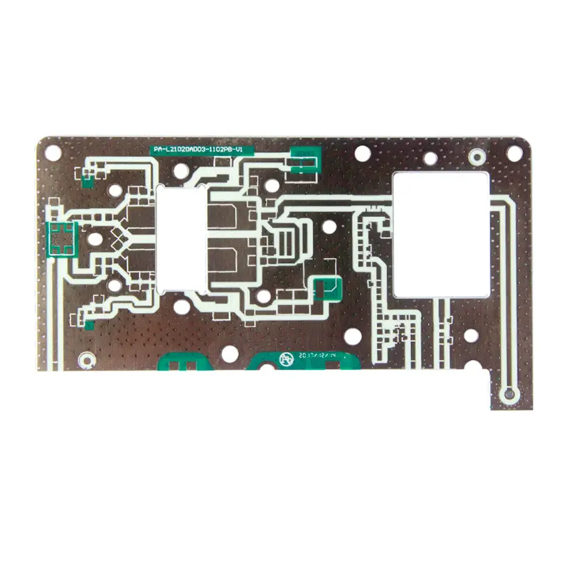
This 8-layer FR4 PCB has a 1.6mm thickness and 1 oz copper. Ideal for antenna designs, it meets IPC6012 Class 3 and IPC-A-600G Class 3 standards, with excellent electrical performance featuring a dielectric constant of 4.2 @ 1GHz and dissipation factor of 0.015 @ 1GHz
| Number of layers | |
|---|---|
| Material | FR4 |
| Board Thickness | 1.6 mm (63 mil) |
| Copper Thickness | 1 oz/ft2 (35 ??m) |
| Quanlity Standard | IPC6012 Class 3, IPC-A-600G Class3, or IPC-6015 |
| Dielectric Constant (Dk) | 4.2 @1GHz |
| Dissipation Factor (Df) | 0.015 @1GHz |
| Applications | Antenna Designs |
| Surface Finish |
Product Overview
This 8-layer PCB uses high-quality FR4 material, with a board thickness of 1.6mm and 1 oz copper, making it ideal for antenna designs and high-frequency applications. The PCB complies with IPC6012 Class 3 and IPC-A-600G Class 3 standards, ensuring its durability and high performance. With a dielectric constant of 4.2 @ 1GHz and a dissipation factor of 0.015 @ 1GHz, it ensures optimal signal integrity for antenna applications.
Product Specifications
Layers: 8 layers
Material: FR4
Board Thickness: 1.6mm (63 mil)
Copper Thickness: 1 oz/ft² (35 µm)
Quality Standards: IPC6012 Class 3, IPC-A-600G Class 3, IPC-6015
Dielectric Constant (Dk): 4.2 @1GHz
Dissipation Factor (Df): 0.015 @1GHz
Application: Antenna Designs
Manufacturing Process
This PCB is manufactured with precision to ensure that all layers are properly bonded and the product meets strict quality standards. The use of FR4 material ensures the board’s strength and durability, making it perfect for use in high-performance antenna designs. The dielectric constant of 4.2 @ 1GHz and dissipation factor of 0.015 @ 1GHz allows for minimal signal loss and optimal performance at high frequencies.
Design Considerations
The design of this PCB is optimized for antenna applications where signal integrity and performance are critical. The use of FR4 material offers stability and reliability in high-frequency environments. With a board thickness of 1.6mm and 1 oz copper, the PCB maintains excellent electrical conductivity while minimizing heat build-up. Designers should consider the specific requirements for antenna performance, including frequency range and signal attenuation, when designing with this PCB.
Applications
This PCB is designed specifically for antenna applications, including communication devices, wireless modules, and other high-frequency technologies. The board’s dielectric properties make it ideal for maintaining signal quality over long distances, and its adherence to IPC quality standards ensures reliability in demanding environments such as telecommunications, aerospace, and defense.
Manufacturing Process and Quality Standards
The PCB is manufactured using advanced techniques to ensure consistent quality and performance. It complies with IPC6012 Class 3, IPC-A-600G Class 3, and IPC-6015 standards, providing high reliability for demanding applications. The PCB’s excellent electrical properties, including a low dissipation factor and high dielectric constant, make it suitable for high-frequency applications such as antenna designs, ensuring minimal signal loss and excellent performance over a wide range of frequencies.
We offer a variety of high-frequency materials, including Rogers (e.g., RO4350B, RO5880), Taconic, and PTFE, depending on customer requirements.
Absolutely, we can provide detailed datasheets for review.
Our high-frequency PCBs can support frequencies up to 110 GHz, depending on the design and materials used.
We ensure precise impedance control through accurate stackup design, detailed impedance simulations, and advanced manufacturing processes.
Yes, we can combine materials like FR4 and high-frequency laminates for hybrid PCBs.
Restrictions mainly involve minimum trace width/spacing and material selection, depending on your design requirements.
We enhance thermal performance by using high thermal conductivity materials (e.g., metal-based PCBs) and optimizing copper thickness.
Thermal conductivity ranges from 0.2 W/m·K to 1.0 W/m·K, depending on the material.
ENIG/Gold Plating/Immersion Silver/Silver Plating/HASL/Gold finger/OSP/Nickel-palladium Gold/Resin plugging/Countersinking/ENIG+Hard Gold Plating/ImNi+ImTin/ENIG+OSP
ENIG is recommended due to its flat surface and excellent conductivity for high-frequency use.
We can produce high-frequency PCBs with layers ranging from 2 to 72.
Yes, we specialize in multilayer high-frequency PCBs and support hybrid stackup processes.
The thickness tolerance is ±0.05 mm, and the trace width tolerance is ±10%.
We perform impedance testing, RF performance testing, vacuum thermal testing, and more.
We achieve this by using high-quality materials, optimized manufacturing processes, and strict control of board thickness and other parameters.
Answer: Prototypes typically take 2–7 business days, while mass production takes 6–15 business days, depending on order volume and complexity.
High-frequency materials (e.g., Rogers) are more expensive, and higher layer counts increase complexity and cost.
We ensure reliability by using high-quality materials, rigorous testing, and optimized manufacturing processes.
Yes, our PCBs can endure temperatures up to 260°C and are suitable for harsh environments.
We use anti-static bags, vacuum packaging, and shockproof padding in the outer cartons for protection.
We provide air freight, express delivery, and sea shipping, depending on your needs, DHL is always prefered that ensure timely delivery through reliable logistics.