- +86 18038188537
- [email protected]
- Mon-Fri 9:00AM - 6:00PM CST, UTC+8
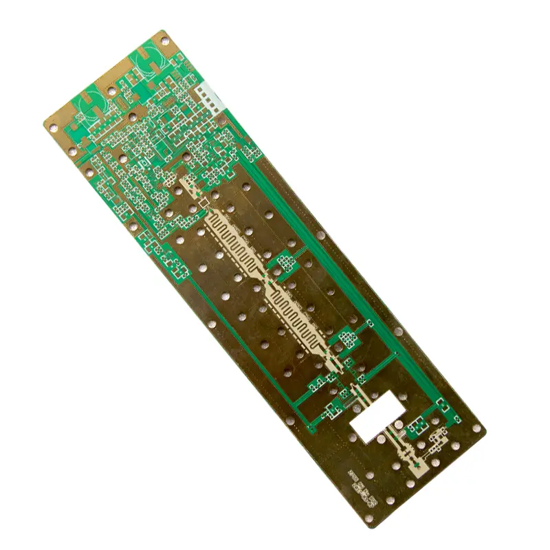
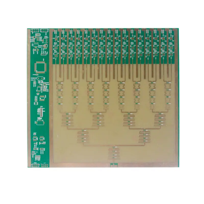
This 12-layer PCB uses Taconic RF-60A material, designed for high-frequency applications such as RF and microwave circuits. It features a 1.6 mm board thickness and 1 oz/ft² copper, ensuring durability and high conductivity. With a dielectric constant of 3.66 and a dissipation factor of 0.0037, the board offers stable signal transmission with minimal loss. Compliant with IPC6012 Class 3 and IPC-A-600G Class 3 standards, it is ideal for demanding applications like 5G systems, aerospace, and high-performance electronics, providing high reliability and excellent signal integrity.
| Number of layers | 12 |
|---|---|
| Material | Taconic RF-60A |
| Board Thickness | 1.6 mm (63 mil) |
| Copper Thickness | 1 oz/ft² (35 µm) |
| Quanlity Standard | IPC6012 Class 3, IPC-A-600G Class3, or IPC-6015 |
| Dielectric Constant (Dk) | 3.66 |
| Dissipation Factor (Df) | 0.0037 |
| Product Type | High-Frequency Sensors |
Overview
This 12-layer high-frequency PCB is engineered with Taconic RF-60A material, chosen for its stable dielectric properties and low-loss performance at high frequencies. The PCB has a 1.6 mm thickness and 1 oz/ft² copper, making it suitable for demanding RF and microwave circuit applications. The dielectric constant (Dk) of 3.66 and a dissipation factor (Df) of 0.0037 ensure minimal signal degradation and stable performance even at high frequencies. The design meets IPC6012 Class 3 and IPC-A-600G Class 3 standards, ensuring reliability for complex, high-speed systems such as 5G communication and microwave technologies.
Material Properties – Taconic RF-60A
Taconic RF-60A is a specialized laminate material designed for high-frequency PCB applications. It provides a stable dielectric constant (Dk) of 3.66 and a low dissipation factor (Df) of 0.0037, which are essential for ensuring minimal signal loss and stable transmission of high-frequency signals. These properties are critical in maintaining signal integrity across multiple layers, particularly in RF and microwave circuits, where signal quality is paramount.
The low Df ensures that there is minimal energy loss during signal transmission, allowing for efficient power usage in high-performance systems. The material’s thermal stability also ensures that the PCB can operate effectively under varying temperature conditions, further contributing to its reliability in demanding environments.
Design Considerations and Layer Stacking
Layer Structure
The 12-layer design is specifically chosen to allow for high-density signal routing and to minimize trace lengths, which is crucial for high-frequency circuits. The PCB is designed with alternating signal layers and power/ground planes to maintain controlled impedance paths, which help to reduce signal reflection and loss. The power and ground planes also provide shielding, preventing electromagnetic interference (EMI) and cross-talk between layers.
The careful stacking of layers ensures that the PCB maintains signal integrity while providing the necessary mechanical support for high-density designs. This layer structure is essential for complex circuit designs, including 5G and microwave systems, where high-speed data transmission is critical.
H3: Trace Width and Impedance Control
Precise trace width and impedance control are crucial for high-frequency PCB designs. The traces are designed to match the required impedance, typically 50 Ω for signal transmission. The width of the traces is calculated based on the PCB’s material properties and the required impedance, ensuring that the signal travels without distortion or reflection. This is particularly important for maintaining high-quality signal transmission in 5G communication and microwave systems.
Manufacturing Process and DFM Considerations
Lamination
The lamination process begins with the selection of Taconic RF-60A material, which is then laminated into multiple layers. Each layer is carefully bonded under controlled heat and pressure to ensure uniform bonding and avoid delamination. This process is critical to the overall performance of the PCB, as any misalignment or bonding issues can lead to signal degradation and loss of performance.
Etching and Drilling
Once laminated, the PCB undergoes an etching process to form the copper traces. Etching must be precise to ensure that the trace width is accurate and consistent. After etching, drilling is performed to create vias for electrical connections between layers. Microvias are drilled using high-precision equipment to ensure that the via diameter is correct and that vias are aligned properly for efficient signal transfer.
H3: Plating and Surface Finishing
Following drilling, the vias are plated with copper to establish electrical continuity. Surface finishing, such as Electroless Nickel Immersion Gold (ENIG), is applied to ensure a smooth surface for soldering and to prevent oxidation. The plating and surface finishing ensure that the PCB has high reliability and durability, especially for high-frequency circuits that require consistent performance over time.
H3: Testing and Inspection
The final manufacturing stage involves rigorous testing and inspection. Electrical testing is performed to ensure that all traces are conducting properly, and there are no short circuits or open circuits. Optical and X-ray inspections check for physical defects, such as poor via plating or layer misalignment. The PCB also undergoes thermal cycling tests to verify that it can handle temperature fluctuations without performance degradation.
Applications
This 12-layer PCB is designed for high-frequency applications that require low-loss signal transmission and high reliability. Key applications include:
5G Communication: The PCB’s low-loss characteristics and stable performance make it suitable for use in 5G communication systems, where high-speed data transmission with minimal signal degradation is essential.
Microwave Systems: The PCB is well-suited for microwave applications, where signal quality and minimal loss are critical for efficient operation.
Aerospace and Defense: The PCB meets the stringent reliability and performance requirements of aerospace and defense applications, ensuring consistent performance under challenging conditions.
High-Performance Electronics: This PCB is also ideal for other advanced applications such as medical electronics, automotive systems, and IoT devices, where high-frequency signal processing is necessary.
Conclusion
This 12-layer high-frequency PCB, made from Taconic RF-60A material, is designed for demanding RF and microwave applications that require stable signal transmission and low loss. The careful selection of materials, design considerations, and precision manufacturing processes ensure that the PCB meets the performance requirements for high-speed circuits used in applications such as 5G communication, aerospace, and advanced electronics. By adhering to strict DFM guidelines, this PCB is optimized for reliable and efficient manufacturing, ensuring high quality and consistent performance across all stages of production.
We offer a variety of high-frequency materials, including Rogers (e.g., RO4350B, RO5880), Taconic, and PTFE, depending on customer requirements.
Absolutely, we can provide detailed datasheets for review.
Our high-frequency PCBs can support frequencies up to 110 GHz, depending on the design and materials used.
We ensure precise impedance control through accurate stackup design, detailed impedance simulations, and advanced manufacturing processes.
Yes, we can combine materials like FR4 and high-frequency laminates for hybrid PCBs.
Restrictions mainly involve minimum trace width/spacing and material selection, depending on your design requirements.
We enhance thermal performance by using high thermal conductivity materials (e.g., metal-based PCBs) and optimizing copper thickness.
Thermal conductivity ranges from 0.2 W/m·K to 1.0 W/m·K, depending on the material.
ENIG/Gold Plating/Immersion Silver/Silver Plating/HASL/Gold finger/OSP/Nickel-palladium Gold/Resin plugging/Countersinking/ENIG+Hard Gold Plating/ImNi+ImTin/ENIG+OSP
ENIG is recommended due to its flat surface and excellent conductivity for high-frequency use.
We can produce high-frequency PCBs with layers ranging from 2 to 72.
Yes, we specialize in multilayer high-frequency PCBs and support hybrid stackup processes.
The thickness tolerance is ±0.05 mm, and the trace width tolerance is ±10%.
We perform impedance testing, RF performance testing, vacuum thermal testing, and more.
We achieve this by using high-quality materials, optimized manufacturing processes, and strict control of board thickness and other parameters.
Answer: Prototypes typically take 2–7 business days, while mass production takes 6–15 business days, depending on order volume and complexity.
High-frequency materials (e.g., Rogers) are more expensive, and higher layer counts increase complexity and cost.
We ensure reliability by using high-quality materials, rigorous testing, and optimized manufacturing processes.
Yes, our PCBs can endure temperatures up to 260°C and are suitable for harsh environments.
We use anti-static bags, vacuum packaging, and shockproof padding in the outer cartons for protection.
We provide air freight, express delivery, and sea shipping, depending on your needs, DHL is always prefered that ensure timely delivery through reliable logistics.