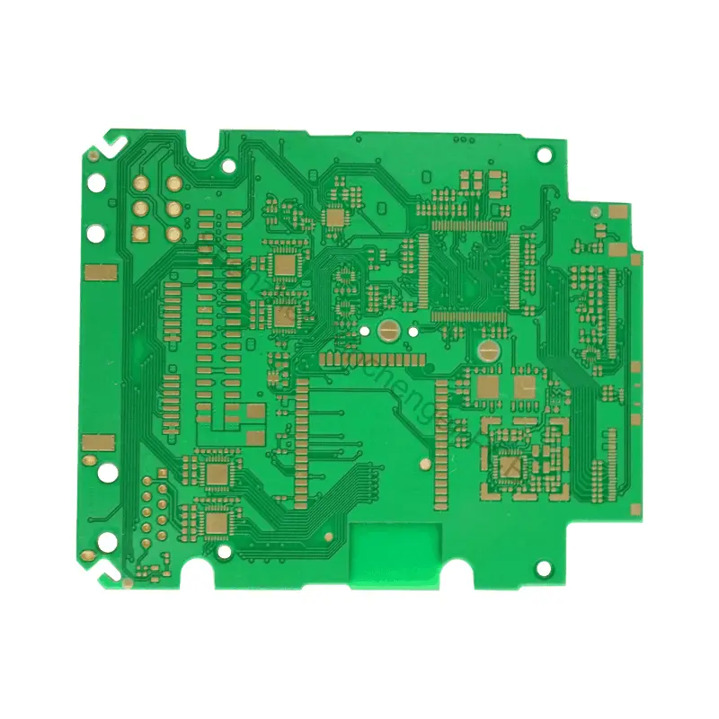
A 4-layer PCB consists of four conductive layers: two outer signal layers and two inner layers, typically for power (VCC) and ground (GND). This configuration enhances signal integrity and electromagnetic compatibility, making it ideal for complex circuits and high-speed applications. The additional layers reduce interference and allow for more compact designs by enabling better routing and power distribution within the PCB.

